The Troubleshooting and Repair for On-board Charger (OBC) Thread

Mitsubishi i-MiEV Forum

Help Support Mitsubishi i-MiEV Forum:

This site may earn a commission from merchant affiliate links, including eBay, Amazon, and others.
Sounds good i will add his link to the index page.

Good pictures of the Laef OBC. i wonder if the IR camera was picking up reflections of the gate drive transformer radiation off of the transistors and other components rather than direct radiation? If the case is 98C then the internal junction temperatures might be near the maximum limits.
 
coulomb said:
Indeed there must be a shunt there.

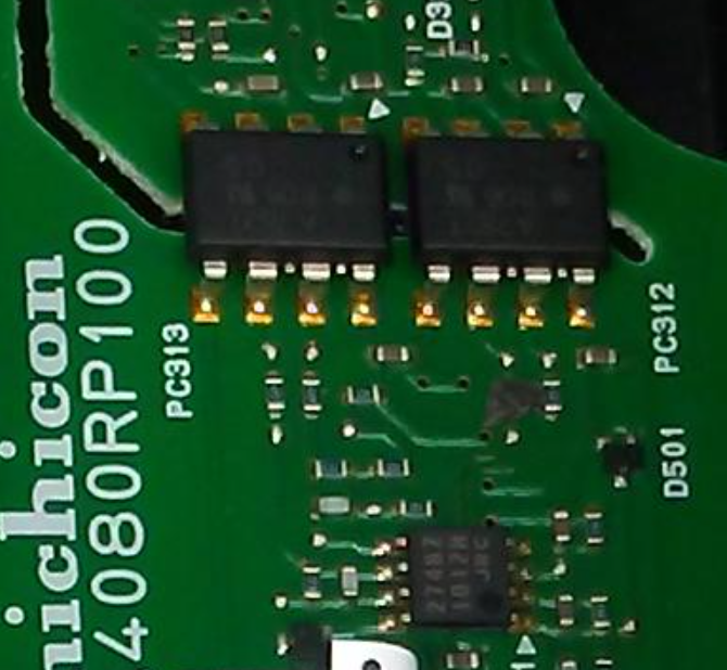
From an earlier CAN bus log, I noted that the DC output current was being reported as 25.5 A, the highest possible value (0xFF = 255 tenths of an amp). Initially I assumed that this was because of my bench configuration, not getting CAN bus packets from elsewhere. But member Kiev reminded me that in the 2012 and later charrgers, there is an 8 mΩ shunt that ends up reporting the current. I then recalled that I'd seen Iout+ and Iout- labels on the output module PCB. So that's the biggest clue so far about what's wrong with this charrger.

Unfortunately, these modules aren't really designed for board level repair, but they're not impossible to service, thanks to pioneers that have shown the way earlier. Thanks, guys! I started removing some of the soft potting compound in the output module, in preparation for desoldering the top board from the bottom module. It soon dawned on me that several of these pins were far too close to the plastic wall that holds the potting compound in place before it sets, so I'd have to remove the plastic wall. This wasn't too hard, although the plastic isn't as strong as I'd like:

file.php


I've tried to superglue it, and it seems to be holding for now. It should be possible to desolder it now; I just need to visit Weber's laboratory to use his desoldering station.

file.php


file.php


R444 and R445 at first glance look like reasonable candidates for the shunt resistor, but alas they are 68 kΩ and are in series across the output to bleed the capacitors after the power is off.

To see if there was the expected 8 mΩ of shunt resistance, I made some measurements of the voltage drops from P0 to POUT and N0 to NOUT. I did this by pushing 3.0 A from my bench dual power supply from one of the transformer inputs to one of the outputs, measuring the voltage after the diodes (P0 or N0) to the output (POUT or NOUT). I came up with 45.4 mΩ on the positive side (so that's PCB tracks plus two inductors), and 53.3 mΩ on the negative side. Subtracting these, I get 7.9 mΩ. Considering the crudeness of this measurement, I'm very happy with this result. It certainly looks like this model has the 8 mΩ shunt.

Meantime, I thought I'd make use of these terminals to test the measurement system:

file.php


I found it strange that there is absolutely no conductivity between the output terminals and any of Vout+, Vout-, Iout+, or Iout-. So on the lower board, there must be some weird isolating amplifier with differential output. It looks like I can just apply 5 V and some current through the negative side and I should see something happening at Iout+ and Iout-. Here is my setup:


file.php


Alas, the outputs measured with respect to MGND:
Vout+: 3.851 V
Vout-: 1.285 V delta: 2.565 V
Iout+: 3.839 V
Iout-: 1.295 V delta: 2.544 V.

Unfortunately, the Iout value did not change at all with applied current. I also tried the positive side, but still no difference.

These seem like very strange voltages to me; perhaps the measurement system is completely broken, or it needs more to make it work. Perhaps 2.500 V represents zero volts and amps, so the measurement can be positive or negative, and only the difference between the outputs is important. It wasn't convenient to put voltage onto the inputs with a third power supply to see if the voltage measurement works at all.

The next step is to find out what's actually down there.
 
That's a good idea to take down the fence.

And some clever testing:
To see if there was the expected 8 mΩ of shunt resistance, I made some measurements of the voltage drops from P0 to POUT and N0 to NOUT. I did this by pushing 3.0 A from my bench dual power supply from one of the transformer inputs to one of the outputs, measuring the voltage after the diodes (P0 or N0) to the output (POUT or NOUT). I came up with 45.4 mΩ on the positive side (so that's PCB tracks plus two inductors), and 53.3 mΩ on the negative side. Subtracting these, I get 7.9 mΩ. Considering the crudeness of this measurement, I'm very happy with this result. It certainly looks like this model has the 8 mΩ shunt.

My guess is that the current shunt will be located in close proximity to the negative terminal of the big electrolytic capacitor.

i can't read the Japanese characters but would guess that they identify the faston tabs, i.e. reference designators.
 
coulomb said:
The next step is to find out what's actually down there.
Kiev, you're going to love this: there is a Viper chip down there! And that part of the circuit burned; photos and details soon.

The Viper chip is SMD and has no heat-sink, but it has the classic 4 pins on one side all connected together.

It seems that this Viper chip provides power on the un-isolated side of the isolating chips. The two isolating chips, with designators PC602 and PC603 (PC for PhotoCoupler?) seem to be Avago ACPL-782T-300E automotive isolating amplifiers, with differential inputs and outputs.

This explains why the measurement outputs did not change with current; the battery-side of the isolating amplifiers requires high voltage from the battery, or at least about 60 V if these Vipers are anything like the ones in the Elcon charrgers.

Sadly, R601 has burned up, and C601 is cracked. C602 beside it and the same size seems to be 100 nF, so I'm hoping that C601 is also 100 nF. These must have a high voltage rating. But I don't know the value for R601. I don't have a 2012+ model here at present. Would anyone know this area of the lower board, and be able to report the value of the resistor near the Viper chip? The Viper doesn't look all that special, just an 8 pin SMD about 3.5 x 4.5 mm, I think it's called an SOT-8 package. The resistor I'm interested in is connected to pins 5, 6, 7, and 8 of the Viper chip, via a small SMD inductor, and the other end connects to battery positive (+360 V).

Thanks in advance for any clues.

Edit: I'm guessing that these might be the equivalent Avago isolating chips. I can almost make out the "A 782T" partial part number (upside down in the photo). The chip below them is the right size for the Viper, but doesn't seem to be one. Pin 1 is on the input side, so the Viper if present would be on that side (at the top of the below photo). This photo is cropped from one on page 1 of this topic, so it's from a 2012+ charrger.

WKOSZhn.png
 
Use of a Viper is amazing and brings back fond memories.

Those circuits have hand sketches for HV sense and current sense. The link is in post #2 on page 1, under schematics and stuff, #7. Here is a direct link to the twisted sister resistor post, https://myimiev.com/forum/viewtopic.php?p=36929#p36929

If this doesn't help i can measure component values if you can mark them on picture.
 
kiev said:
Those circuits have hand sketches for HV sense and current sense.
Ah, I'd forgotten all that; thanks for the reminder and pointers. I think I still have some 39 k M1608 resistors here from that time.

If this doesn't help i can measure component values if you can mark them on picture.
Unfortunately, it looks like these two charrgers use totally different ways of powering the un-isolated side of the isolation amplifiers. 2012+ seems to use transformer T302, powered from the auxiliary battery, whereas this 2010 is using the Viper and some sort of buck converter from the high voltage battery.

I'm pretty sure that no-one else has gone to the trouble of getting to this board, and it's a fair bit of work. So I'm going to have to trace out the circuit, and calculate a reasonable value for R601. I'll likely replace it with a larger one so that it hopefully lasts well. It looks like the circuit is pretty similar apart from the power supply, albeit with part of the circuit split between the output module and the control board. But my guess is that it's only the power supply that is faulty.

Then I have to figure out a replacement for the white goo. I was hoping that it would come out in more or less one big lump, but it ended up in hundreds of pieces. It needs to be thermally conducting, electrically insulating to hundreds of volts, and able to be roughly shaped. Any suggestions on that front are very welcome.

That brown gunk I was worried about several posts ago seems like it was just flux trapped by the white gunk. They possibly needed the flux for the thick inductor wires.
 
I'm pretty sure that no-one else has gone to the trouble of getting to this board, and it's a fair bit of work.
That's true but you are the only one over there who could dig this deep and solve the problem.

re: White thermal pad,
Cho-Therm pads are a good solution and might be what was used.
https://www.digikey.com/en/product-highlight/p/parker-chomerics/cho-therm-1671-high-power-electrical-insulator-pads
 
coulomb said:
So I'm going to have to trace out the circuit, and calculate a reasonable value for R601. I'll likely replace it with a larger one so that it hopefully lasts well.
Or not. According to this application note, that resistor acts as a fuse. It looks like 10 kΩ 0.25 W might be suitable, and hopefully the exact value is not critical.
 
coulomb said:
And that part of the circuit burned; photos and details soon.

This is what's under there, with the top board unsoldered:

file.php


With the white gunk removed:

file.php


How the connections are wired:

file.php


Resistor R601 and capacitor C601 were damaged. I need to figure out what value R601 is, since it was burned beyond recognition. The schematic for the power supply portion:

file.php


Edit 2023/Aug/03: Changed the connection diagram slightly. New parts are in blue.
 
i wonder why the fuse resistor and capacitor blew?
Is the voltage regulator chip damaged, there appears to be some strangeness to its surface and some darkness on the pcb across the diode to the damaged cap and resistor--maybe its just flux residue or ?

Could the fuse resistor be like the second application, 10 Ohm 1/2 W ?

Where did they put the 8mR current sense resistor?

The white gunk looks more like an injected mixture rather than a co-therm pad.
 
I have the same problems.
https://imageup.ru/img57/4455174/img_20230801_205554.jpg.html
https://imageup.ru/img289/4455178/img_20230801_205535.jpg.html
 
Good job Vik, well done to remove that board.

Can you read the markings on R601 or measure its value?

Same with capacitor C601, although cracked it may still give a value when measured.

Is the voltage regulator chip, IC602, cracked or just scratched?
 
kiev said:
i wonder why the fuse resistor and capacitor blew?
It's a worry. I suspect that chip ceramic capacitors aren't very good long term with high voltage. Hence the snubber caps on the daughter boards failing spectacularly. So I think I'll replace C601 and C602 with leaded capacitors, if I can fit them safely.

Is the voltage regulator chip damaged,
Hard to be sure, and I haven't checked for shorts yet. I'll buy a replacement anyway.

Could the fuse resistor be like the second application, 10 Ohm 1/2 W ?
Yes, it could. So that narrows it down to just four decades of resistance :eek:

Where did they put the 8mR current sense resistor?
I haven't found it! I suspect it's under the board at the bottom right. I've also not found the diode that is necessary for a buck converter, though I can measure its forward voltage drop. Also, the voltage outputs have 100Ω of resistance between the isolator chips and the PCB edge connectors, so there must be resistors under the board as well. It looks like it would be a royal pain if I had to remove that board. My guess is that components on the under side would get stuck in the potting and be damaged when the board comes off.

The white gunk looks more like an injected mixture rather than a co-therm pad.
It looks to me that it comes out as a thick tube and gets squashed flat as they assemble the top board to the base. A bit like a run of toothpaste except more viscous and perhaps 20 mm diameter.
 
coulomb said:
Kiev said:
Could the fuse resistor be like the second application, 10 Ohm 1/2 W ?
Yes, it could. So that narrows it down to just four decades of resistance :eek:
I've decided that using a resistor as a high voltage DC fuse is not a great idea. So I'll use an SMD fuse. Alas, these are 11 mm long, so they won't fit on the PCB. I'll mount them and two ceramic capacitors Christmas tree style to the right of the board.

[ Edit: Mouser and Digi-Key are out of stock of suitable fuses at present, but I found that Element 14 have Eaton fuses in stock, and those are cheaper as well. ]

I'd like to use a single layer ceramic capacitor for C601 and C602, as I assume that these would be the most robust. But these are 23 mm diameter, two would not fit in there. So I'll compromise with multilayer ceramic but leaded, again Christmas tree mounted to the right. These are possibly no more reliable than multi-layer SMD types, but they seem more robust to me. Also, I can get them with automotive ratings.

Kiev said:
Where did they put the 8mR current sense resistor?
I haven't found it! I suspect it's under the board at the bottom right.
I have slightly more evidence that it's between the four pins that go from bottom to top near the bottom right. I messed up before; two pairs of these sturdy pins connect to each other, but only one voltage sensing pin is on the PCB. So that makes it seem unlikely that the resistor is on the back of the main PCB. Probably it's on the lower PCB that carries the diodes and other heavy current tracks. That PCB possibly has double or more thickness compared to standard PCB tracks.
 
I've decided that using a resistor as a high voltage DC fuse is not a great idea.
i was somewhat disturbed seeing a fuse resistor in the application note. You are right to do something different. Part of the problem is access if the circuit fuses again, in addition to the problems of dealing with HVDC. A fuse resistor might be ok for a laboratory bench prototype circuit used for development, but not so much in production.

The board shown by vik013 had cracked ceramic capacitors too; those things are ELB, evil little basterdges, prone to cracking and causing intermittent faults. Troubleshooting is a nightmare In this case with the hidden board under the thermal toothpaste.
 
kiev said:
i was somewhat disturbed seeing a fuse resistor in the application note.
Agreed!

You are right to do something different. Part of the problem is access if the circuit fuses again, in addition to the problems of dealing with HVDC.
This circuit would presumably be active any time that the battery contactors are on, not just while charging. So you really don't want tiny PCB parts, especially ELBs ( :D ) powered with full battery voltage every time that you're driving, without decent protection.

I'm a little concerned that these SMD fuses can only clear 100 A, but it has to be better than a smallish SMD resistor that's not designed to quench a DC arc. I'm sure that the wiring would have 3.6 Ω of resistance. But the fuse in the motor controller will clear any disaster current. Presumably these ceramic capacitors don't typically fail dead shorted.
 
ctromley said:
Mine weren't as bad as yours. (Are those solder balls on the contact pads of yours?) What I found with mine is that the contact pads are not adhered to the flex, so they probably snagged on something by handling.

Thanks for the detailed explanation!

Concerning the flat ribbon cable, I think on the picture it looks worse than it is. They are just bent, but the shadow and light on the picture make it look like there is something on the pads.

I have another question for the people on this forum. Does anyone know where to get the right thermal paste to apply to the bottom of the waffle plate? Most of the ones I found are for CPUs.
 
From a quick search i found this Dowsil TC-5860 that has a high thermal conductivity. Other than being gray in color it seems like a good candidate.
https://www.dow.com/en-us/pdp.dowsil-tc-5860-thermally-conductive-compound.517744z.html?productCatalogFlag=1#tech-content

The heat plate inside the OBC appears to be machined to a very shiny and mirror-like finish, whereas the bottom of the waffle plate is just a plain mill finish. In both cases there will be microscopic voids, grooves and tool marks in the surface finish, plus there can be waves in the surface figure (not perfectly flat).

From wikipedia, the thermal conductivity of air is on the order of ~0.03, thermal grease is ~0.4 to 3, and aluminum is ~100 to 200 depending upon purity.

So the best heat transfer would be for a metal-to-metal contact such as in a lapped surface, but the tool marks cause a microscopic gap between the surfaces, and the thermal compound is intended to fill the air gaps and transfer heat from the hot surface to the cooler.
 
Interim pictures of the output module repair. It's not tested as yet; I need to organise some power supplies.

This was my first attempt at laying out the parts:


file.php


I then realised that there was enough room to mount the capacitors directly on the PCB, and that this would probably result in better spike suppression performance, or at least similar to original performance:


file.php


Those are TDK 100 nF 630 VDC capacitors, and a 1 A fast blow 500 VDC fuse.

Once tested, the parts will be siliconed and the boards conformally coated.

Edit: I've since added a 150Ω ceramic composition resistor in series with the fuse. As noted below, the correct value would have been 330Ω, but I had the 150Ω in stock for Elcon charrger repairs.

file.php
 
coulomb said:
It's not tested as yet; I need to organise some power supplies.
It tested fine; 16.0 V at the input to the voltage regulator, and 5.0 V out. This was with 52 V at the input of the power supply (representing the battery voltage). Now to put it all back together. It drew some 6 mA, for just over 300 mW. At more realistic battery voltages, it would presumably draw about one milliamp.
 
Back
Top