The Troubleshooting and Repair for On-board Charger (OBC) Thread

Mitsubishi i-MiEV Forum

Help Support Mitsubishi i-MiEV Forum:

This site may earn a commission from merchant affiliate links, including eBay, Amazon, and others.
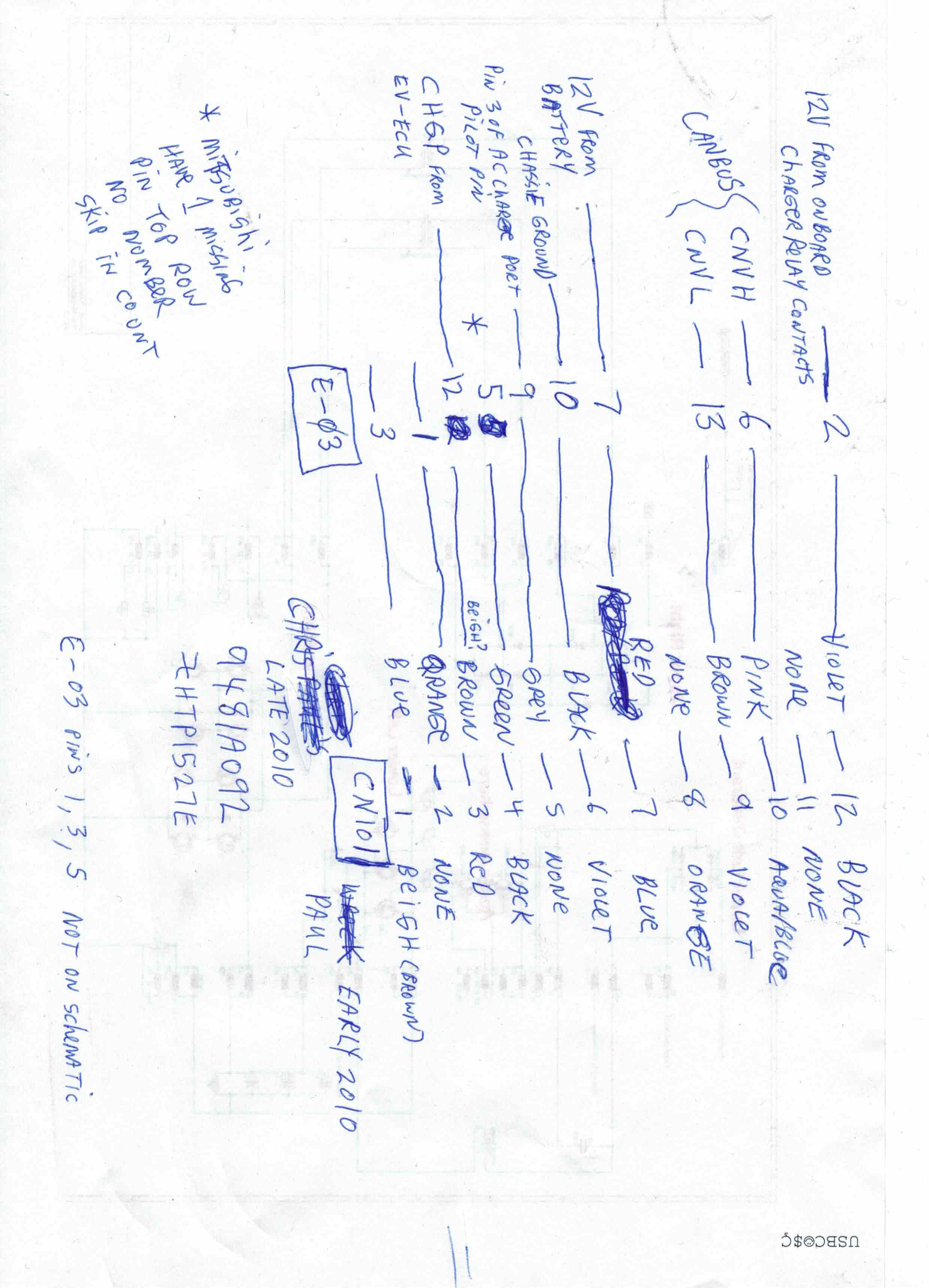
Here is a drawing showing the signals from the rest of the car through the E-03 Connector outside of the charger box, to the CN101 Connector that plugs onto the top PCB. I have two chargers, one a Late 2010, and one an Early 2010.
The CANBUS Comes in on E-03 pins 6 and 13 and runs to CN101 PINS 10 and 9.
One differences between the two versions of 2010 Chargers are Pin 2 of CN101 Is a orange wire in the Late 2010, while Pin 8 is the orange wire on the Early 2010 (moves from top to bottom row of connector)
One strange thing is that the 12v supply from the battery on pin 2 of E-03 connects to CN101 PIN 12 which is a violet wire on the Late 2010 model but the scary bit is that this 12v supply connects to a black wire on the Early 2010 charger.
Pins 1,3, and 5 do not show up on the Maintenance manual schematics.

So connecting 12v to CN101 Pins 12 and 7, and connecting ground to Pin 6 of CN101 Should power up the PCB.

The remaining question is what to do with the CHGP signal CN101 PIN 3 (E-03 PIN 12) which connects to the EV-ECU. Not sure if this is a input or an output signal.
Also Pin 9 of E-03 ( CN101 Pin 5 ) is a Grey wire on the Late 2010 version that connects to PIN 3 of the AC Charging port.
I'm not sure if this is the Pilot Pin or the Proximity pin. In the Early 2010 Charger, this wire is not populated in the connector.

vqxioTr.jpg
 
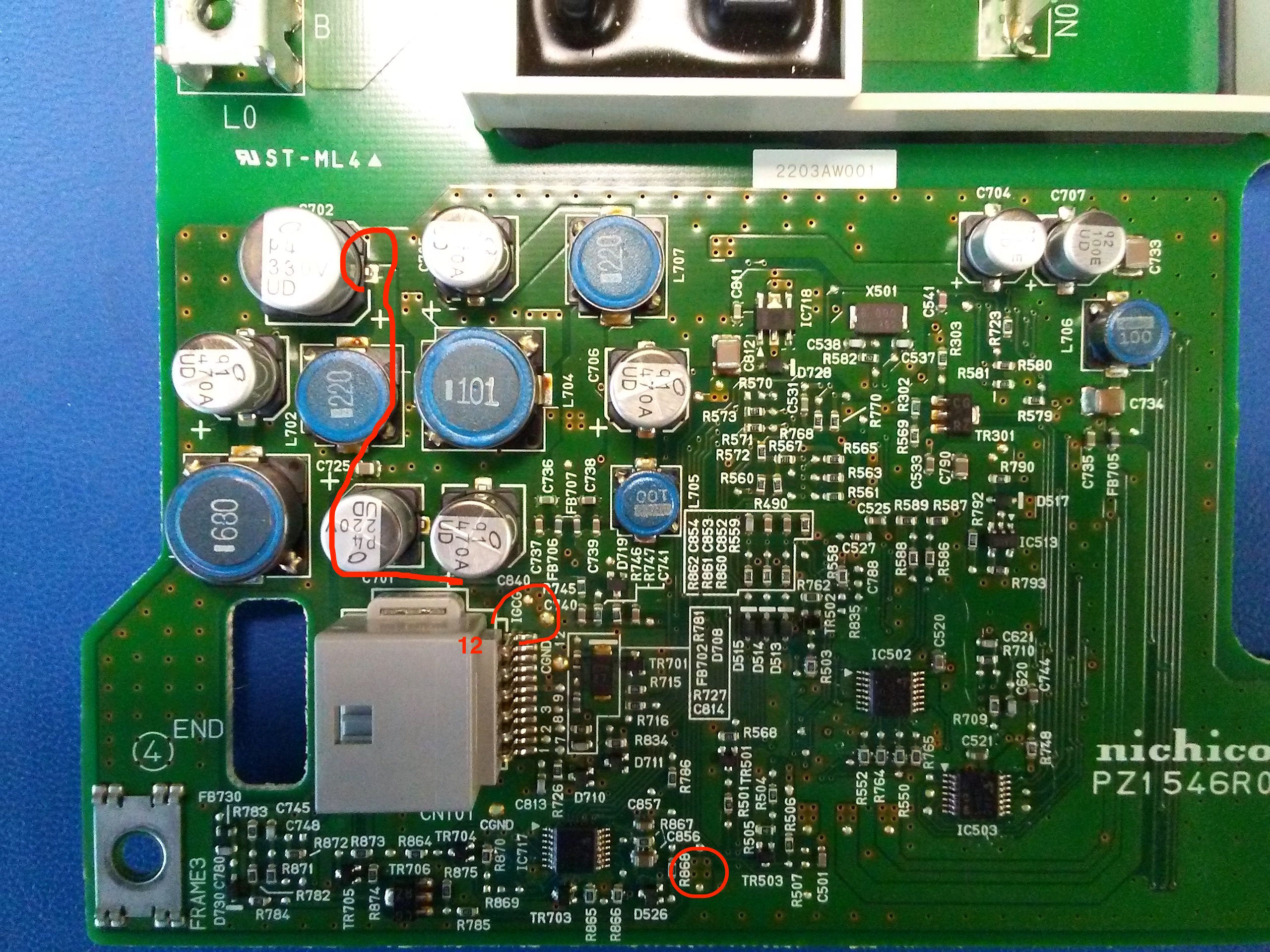
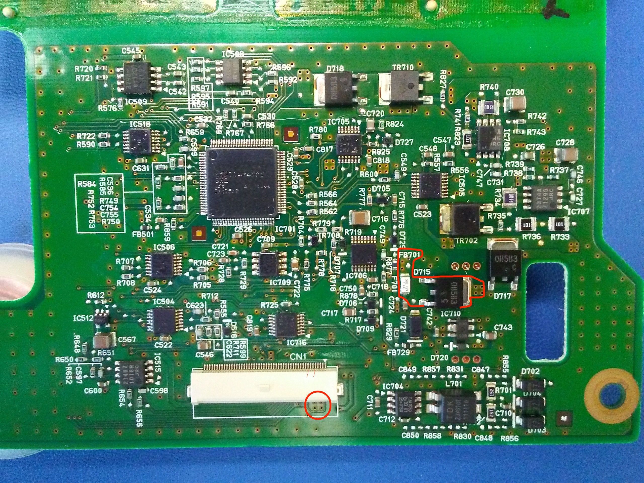
The control board, aka top board, is a multi-layer construction with internal traces.

It appears that a 12V supply power enters on pin 12 of the control board, is filtered by caps and coil, then passes thru a 4A fuse and a barrier diode before exiting on pins 5-8 of CN1 to provide 12V supply to the bottom board.

top layer
jnytOPJ.jpg


bottom layer
ej5HWf0.jpg
 
@sky, great job on tracing the cable and noting the differences.

Looks like the 12V supply for the bottom board is thru the relay and is switched on by the EV-ECU, so part of troubleshooting would be to verify that the relay is coming on and 12V coming to the box.

http://mmc-manuals.ru/manuals/i-miev/online/Service_Manual/2012/54/html/M154950190002101ENG.HTM

How about that fuse check for continuity?
 
When I first checked the fuse, I thought it was blown, but then I scratched the end/pads because they looked like conformal coating,
and once I cleaned up the end, it showing 0R so the fuse has not been blown on my unit. That conformal coating can throw you off if not cleared off.
 
[edit] But first, does your top control board(s) look like the same general layout as the one i posted?

i think if you are careful you could verify that 12V is coming in to the control board on the 2 supply lines, the one that is powered all the time and the one from the relay contacts. The switched power could be measured at the little test point near the 4 vias circled in red near the bottom of the picture of the control board top layer posted above. If no voltage there then the bottom board is not getting 12V power.

Your measurement between pin 3 and the tab of TR310--was that a dc measurement or ac on the scope? If working properly then that signal would be pulsing between 12V and ground at the pin 1 gate frequency coming out of IC702 on the bottom side, the flyback switching regulator chip. If the regulator was not working and 12V was getting to the bottom board then i would expect to read 12Vdc.
 
Hi KIEV:

Yes, my TOP Board appears to be same Version/revision as your picture.
Starting with the charger on Bench with nothing else connected, I've made up a cable and I'm supply 13.0v from a motorcycle battery to Pins 12 and 7 of CN101 with ground connected to pin 6.
I still have the wires soldered to the TAB and PIN 3 of transistor TR310 on the bottom PCB, and I am measuring 12.66v there between these points. I am also measuring 211ma from the 12v supply battery.
On the top PCB, I've also measured the following voltages across the electrolytics:
C702: 12.52V
C706 5.18V
C707 16.75V
C704 16.75V
C737 5.19V
C701 12.46V

while having the 12v battery connected to the pin on the CN101 Connector, I've also tried applying 240vac to the mains screw terminals on the top pcb, and checked to see if there is any AC at the primaries of the transformer that are on the ouptus of the IGBT's. This is still dead.
We probably need to work out what signal needs to be on the CHGP Line from the EV-ECU to pin 3 of CN101. This is probably the signal that actually enables/disables the running of the IGBT's.

I'm also having problems working out the The PE and CP Proximity and Pilot pins from the j1772 connector to the charger for bench testing.
I think that PIN 4 of the J1772 is an output to EVSE to tell it what charge status is on car based on change in resistor values. This was not fully implemented on 2010 I-MIEV, and since it's an output, it not required to get charger enabled for bench testing.
Pin 5 on the J1772 is the proxiity pin that confirms the charger cable is plugged in. I think this pin connects to ground when a charger cable is attached. If this is true, then this would connect to pin 9 of connector E-01 which in turn connects to pin 5 of the CN101 Connector on the TOP PCB. It looks like this pin is not connected on the early 2010 model, but is connected in the late 2010 model.
I think this would mean that Pin 5 of CN101 would need to be connected to ground before the charger would run.
Kiev / Coulomb: do you have any info on this to confirm this?
 
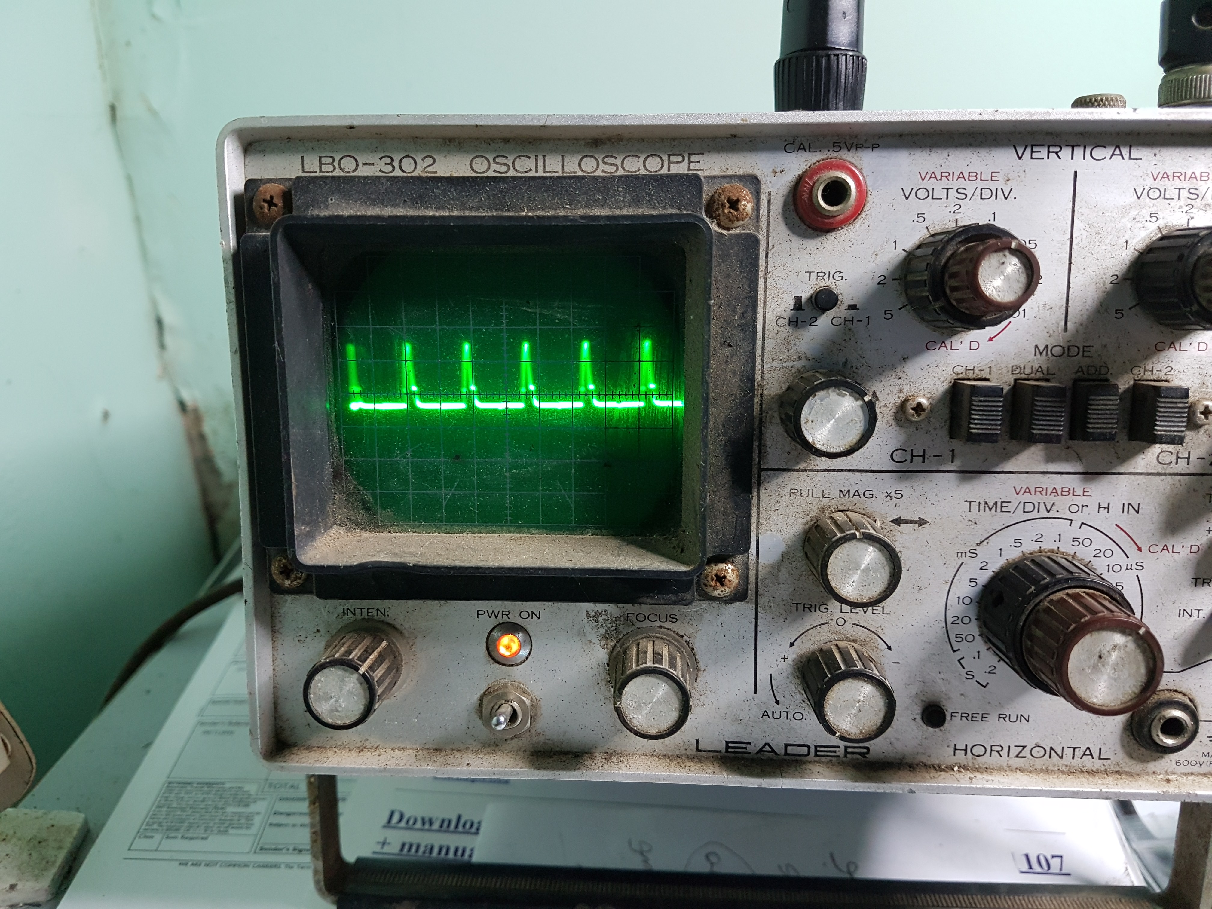
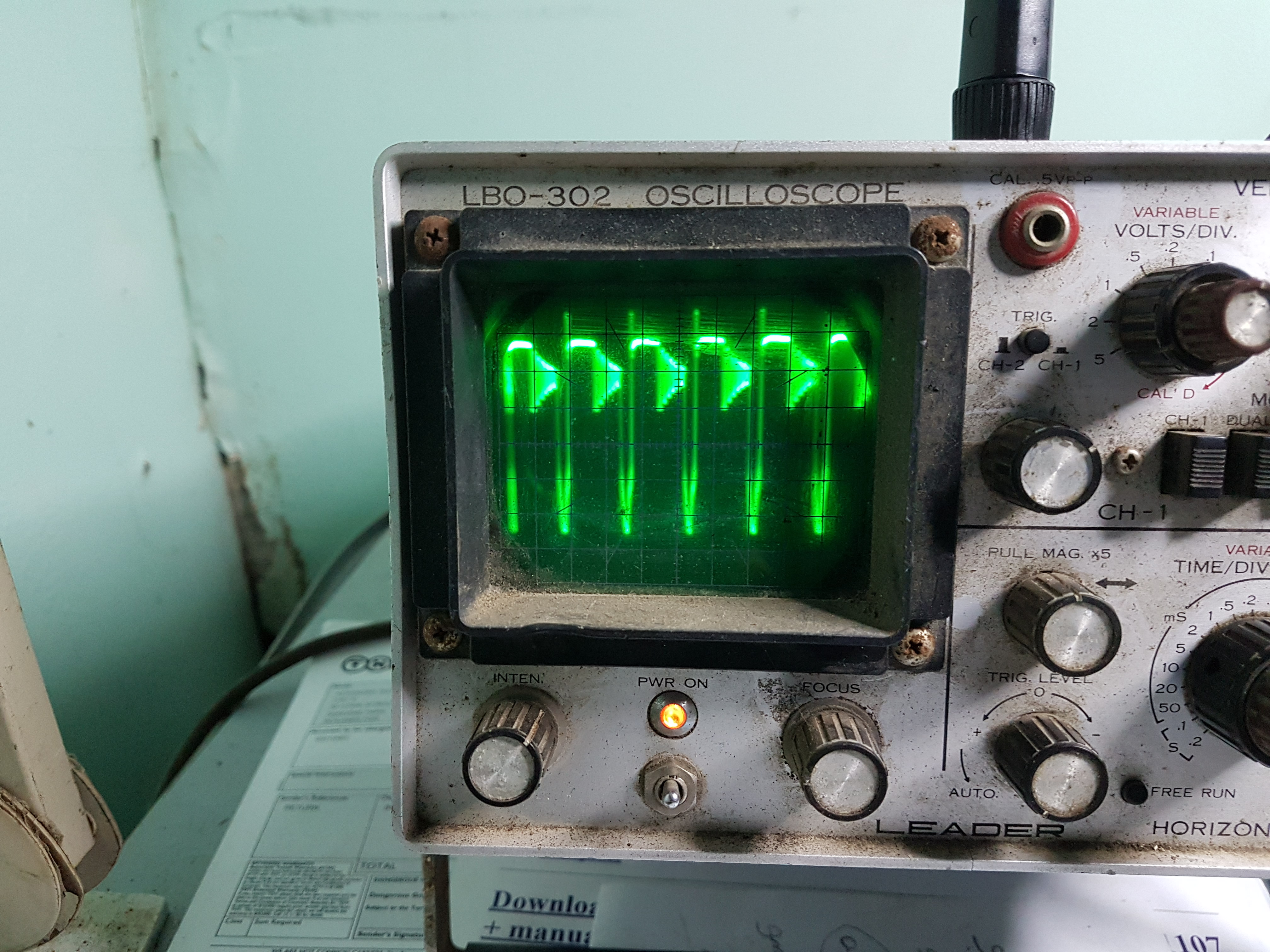
I finally got things setup to look at the pins of TR310 on the bottom board with the scope:


bVRRIKV.jpg


IBFgEui.jpg


So this looks like TR310 is chopping ok, now I need to pull it apart and find out what test points to test for the other supplies.
 
skylogger said:
C707 16.75V
C704 16.75V
Huh. So something is boosting the 13 V input, or else there are some spiky signals confusing the multimeter. But across large capacitors, this should not be the case. It seems such a non-standard value. And so unnecessary given that there is another power supply chopping it up on the next board. It's possible that it's meant to be some other value, say 20.0 V, and some fault is loading it down, but for now I think we assume it's meant to be "about 17 V" until proven otherwise.

... checked to see if there is any AC at the primaries of the transformer that are on the ouptus of the IGBT's. This is still dead.
This is to be expected, considering we still have about three other balls to juggle.

We probably need to work out what signal needs to be on the CHGP Line from the EV-ECU to pin 3 of CN101. This is probably the signal that actually enables/disables the running of the IGBT's.
Yes, this is the first one. I note that the proximity signal from the J1772 connector (that Mitsubishi are calling pin 4, but the rest of the world calls pin 5) goes straight to the EV-ECU. So when the user presses the button (meaning stop charging, I believe, but I'm no J1772 expert as yet), this must go via the EV-ECU and the only ways to stop the charge are via the CHGP signal, or by cutting the power to the charger relay. The latter seems way too crude to me; you want to gracefully shut down the power, after immediately cutting off gate drive to the main IGBTs to stop charging. Otherwise, you could have IGBTs with partial gate drive going into linear regions and overheating.

I'm also having problems working out the The PE and CP Proximity and Pilot pins from the j1772 connector to the charger for bench testing.
I think that PIN 4 of the J1772 is an output to EVSE to tell it what charge status is on car based on change in resistor values. This was not fully implemented on 2010 I-MIEV, and since it's an output, it not required to get charger enabled for bench testing.
My understanding is that proximity is a signal to the vehicle, so it can tell one of three states: no plug connected, connected but button not pressed, and connected with button pressed. You might measure the voltage to chassis at the proximity pin; not connected should be 4.5 V due to a 330 Ω pullup to 5.0 V and the 2.74 kΩ pulldown near the J1772 socket. If so, try putting a 150 Ω resistor to chassis so that the pin falls to 1.5 V. You might consider putting a switch in series with that resistor, perhaps a normally closed one, with a 330 Ω resistor across that switch. Then if something goes wrong, you press that switch in a hurry, and it's like pressing the J1772 plug button, which I believe should kill the charging. Maybe even make it a red mushroom type (an E-stop for charging).

Pin 5 on the J1772 is the proxiity pin that confirms the charger cable is plugged in. I think this pin connects to ground when a charger cable is attached.
Again, my understanding is that when the cable is attached, that pin 5 (according to the rest of the world, or pin 4 on the Mitsubishi diagram) needs 150 Ω to ground to indicate cable presence. A short circuit to ground would be 0 V, an error, and would likely prevent charging.

Pin 5 on the Mitsubishi diagram is the large earth pin at the bottom, which the rest of the world calls pin 3. Some diagrams show it as neutral in split phase situations, but fortunately you don't have that. All the diagrams I see show the vehicle connecting it to chassis / earth / ground. This seems to be the reference for the pilot and proximity signals.

I note that the pilot signal is generated by the EVSE, and "read" by the charger, although the charger modifies its amplitude with a diode and two different valued resistors. It might be necessary to generate a ±12 V 1 kHz square wave (24 V p-p) with a 1K resistor in series to keep the EV-ECU happy. It might be necessary to start with DC +12 V to initiate the handshaking (state A, EVSE ready, not connected).

If this is true, then this would connect to pin 9 of connector E-01 which in turn connects to pin 5 of the CN101 Connector on the TOP PCB. It looks like this pin is not connected on the early 2010 model, but is connected in the late 2010 model.
I'm confused. Pin 9 of E-01 connects to pin 3 of the J1772 socket per the Mitsubishi diagram. This seems to be the pilot signal, that the rest of the world calls pin 4. It makes sense if these are not connected in early 2010 models, since they don't do real J1772 charging, and merely connect the mains (large pins 1, 2) to a mains plug (forgive me if I got this wrong). I thought all Australian 2010 models are like this, unless or until they have the "Gelco" modification, which makes them more or less proper J1772 compliant, so you can charge at public charging stations. @Skylogger, has your 2010 had the "Gelco" modification done? Does yours connect to the pilot signal (rest of the world pin 4, Mitsubishi pin 3)?

I note that the confusion re pin numbering is merely the number that's the problem; the function (e.g. line / pilot / proximity / protective earth) is the same, as it needs to be to work with public charging stations.

I think this would mean that Pin 5 of CN101 would need to be connected to ground before the charger would run.
Kiev / Coulomb: do you have any info on this to confirm this?
As above, I disagree, but am happy to be proved wrong.

[ Edit: "no button" -> "button not pressed" ]
 
That is some good data on the cap voltages, and a great capture with the scope. That proves out quite a bit of stuff that is working, and every little bit helps solve the puzzle.

As Coulomb said there are several balls to juggle here before even being close to getting a charger to run on the bench. Here is my list:

1. CAN buss commands from the EV-ECU. The voltage and current commands are calculated and determined by the EV-ECU with data from the BMS and Cell Monitoring boards. There is a big ole processor chip on the underside of the top board that receives these commands and implements the necessary detailed control commands for the PFC and FETs, etc. i'm sure it won't work without this.

2. The J1772 protocol implementation (or not), probably a minor issue.

3. Troubleshooting the box to determine what has failed and why, and what else might also be damaged besides the obvious burned resistors or blown snubber caps. Why did they fail, what caused the chain of events to create the damage, etc. This is important to prevent repeating or causing futher damage.

4. The top board creates multiple power supply voltages, the bottom layer has the processor and a multitude of CMOS logic chips, plus any sensor and signal conditioning needed to provide data to the microprocessor. The bottom board is simple in comparison. We have to know what is normal operation to compare for troubleshooting.

5. Diagnostic Trouble Codes in the EV-ECU. Some codes will prevent the OBC from operating, so the codes need to be read and cleared if possible.

i did the easy part (bottom board) first because i've been bullriding in this rodeo before. It does take a lot of time to trace it all out, but i don't know of any other way to get the knowledge . You've got the best team working on this including the master boomerang thrower of all time in QLD--coulomb has special skills and magic with processor code.
 
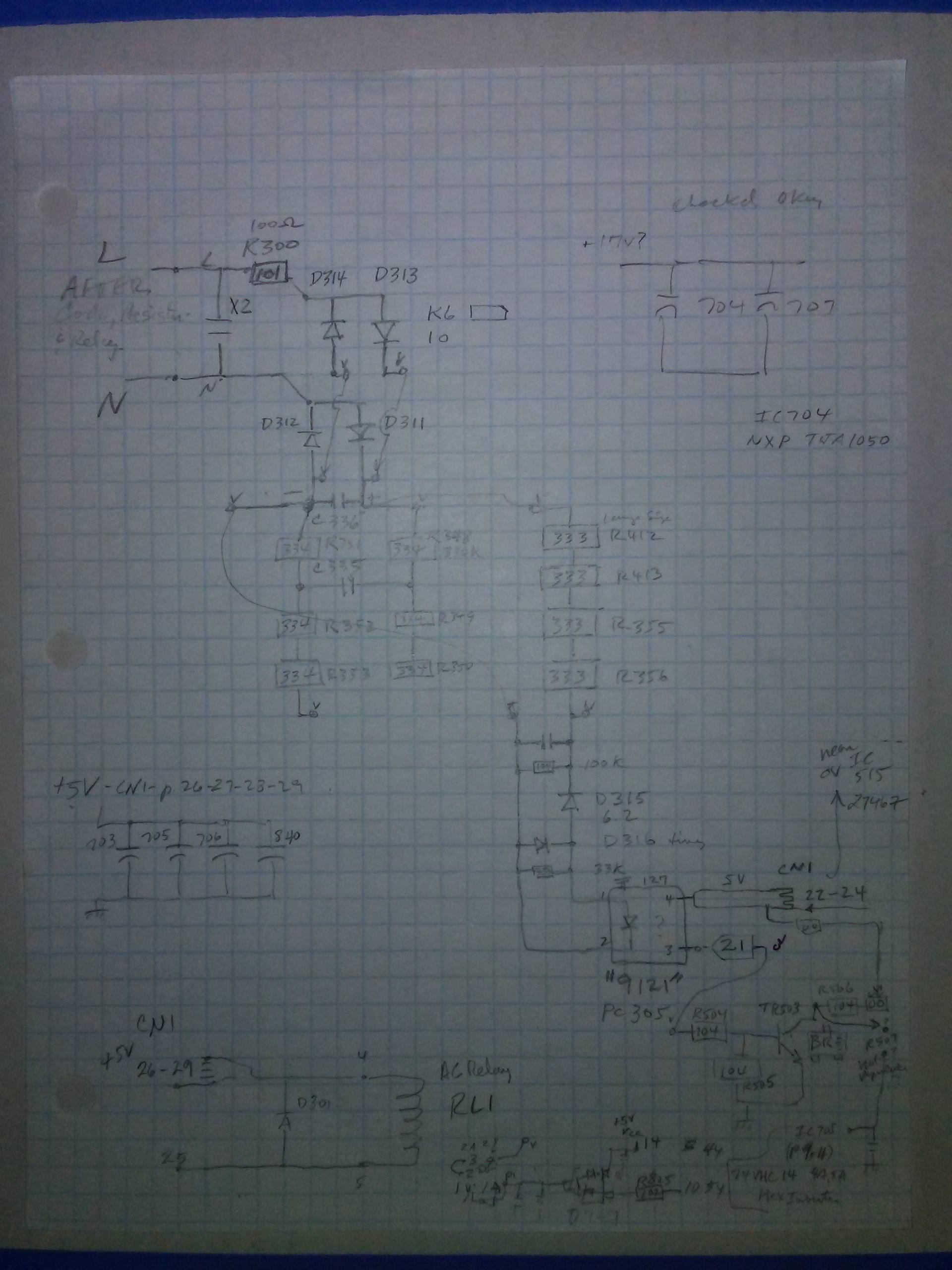
i found a small diode rectifier bridge circuit on the bottom board coming out of the side of the AC input doghouse. It runs thru a series string of resistors to drop the voltage way down, then gets passed to an optocoupler and sent up to the top board. i expect that it goes to the microcontroller to provide a signal that AC is present in the doghouse, and that the relay, emi filter coils, and resistors are good. i traced the top board portion and rang it all out except for the final link to the processor pin--i'm sure it must be there but the multilayer board and tiny parts and traces are a real pain...

The 12V supply that is hot all the time Pin 7 of CN101, creates a 5V supply on the top board (and possibly more) that is used in this AC sense circuit on the bottom board. If possible try to repeat your test and measure the current draw with just that one 12V to the board with the CN1 cable attached to the bottom board. And measure the cap voltages. i suspect that only a portion will be energized and it would be good to know what the "OFF" state power draw of the OBC might be.

Thanks to your capacitor voltages i now know where to look on the top board to flush out the low voltage power supplies--that will save quite a bit of time.

i have hand written notes for this and will convert to schematics as time permits.

p.s. i checked the wiring colors in Jay's box and it matches your late 2010 colors. One of the brown wires with the CAN line is dark brown, the other is lighter such as tan.
 
kiev said:
That is some good data on the cap voltages, and a great capture with the scope. That proves out quite a bit of stuff that is working, and every little bit helps solve the puzzle.
I totally agree; thanks @Skylogger.

It does take a lot of time to trace it all out, but i don't know of any other way to get the knowledge .
That "lot of time" is greatly appreciated, Kenny.

You've got the best team working on this including the master boomerang thrower of all time in NSW--coulomb has special skills and magic with processor code.
QLD (Queensland, the sunshine state), actually. Just north of New South Wales. I'm happy to lend my processor code skills if I get the opportunity, but we were pretty lucky last time (with the Elcon/TC chargers) to get our hands on the charger firmware to work on. Firmware is usually pretty well protected. Another way to access the code is through the firmware updates, if there are any. But it seems that these are kept in Mitsubishi's hands, and never let into the public domain, is that right?

And thanks for the kind words.
 
i traced out the CHGP pin, pin 3 of the CN101 connector on the top board. It appears to be an OUTPUT from the OBC to the EV-ECU.

There will be 3 inputs to channel 2 of IC706, Toshiba 74VHC123A, a monostable multivibrator chip. If any of the inputs make a transition, H->L, or L->H, then the chip outputs a short pulse. This pulse drives the base of an NPN transistor, which pulls the output at pin 3 Low, which is the CHGP wire running to the EV-ECU.

Maybe this is a protection signal?

q44TPYT.png
 
[EDIT]: Just as I posted this, I just noticed KIEV has just traced out the same CHGP Signal, so my post is a bit redundant.

I've just made a discovery by accident. All of the below checking is with charger out of the car.
I measured the resistance between the Earth Ground Pin, and the Proximity pin on the Gun end of the cable.
When the Trigger is pressed opening the connection just before plugging onto car, I measure 480R.
When the trigger is released (connection closed with gun fitted to car) I measure 150R resistance.
This all confirms what Coulomb ways saying earlier, so it appear to make things happy, a 150R value needs to be present on this line.
This I believe would be the change in resistance that would be presented to the CNCT Signal on the EV-ECU Connector C111 pin 103.
So for Bench testing this signal does not need to be emulated as input to the charger, just the resulting signal from the EV-ECU or relay switching that would result. While I had the charger cable connected, I was using Ohm meter to check between pins on the E-03 Connector that connects to the charger.
To my surprise, when I connected the Ohm meter across pin 10 (Ground) and PIN 12 (CHGP from EV-ECU) The OBC Relay switched on, you could hear the fans start, and the charging light started blinking on dash (and of coarse the Triange with !) since there was no charger installed at the time.
From this, I would suspect that the CHGP signal is an Output from the Charger to the EV-ECU. The voltage from my Ohm meter would have been seen by the EV-ECU to look like a signal from the charger. The EV-ECU then applied a pull down to it's CHGB pin 66 which activates
the A-06X On Board Charger relay. This means that since the CHGP is an output from the Charger, it's not required to get the charger running on bench testing, as long as 12v is applied to Pin 12 of CN101 to simulate the OBC Relay switching on.

As a side note, When this charger was previously in the car, and the charger cable was connected to the car (with 240v supplied)
The OBC Relay would come on, You would hear the cooling fan come on, The charge light would flash on the dash, and the Triangle with ! on dash would also come on, then after a few seconds the fan and charging dash light would go out. This is exactly what happens in the testing above. So this makes me think the Charger is also generating the CHGP signal to the EV-ECU.

Also note the car being used is a wrecked 2010 I-MIEV for use as a test bed, and all of its electronics were working 100% before charger removed. The good charger was taken out and used as a replacement in another car, and the broken charger is now on bench for testing.
This means any testing results with the broken charger put back into this wrecked I-MIEV are known to be results of the faulty charger and not any additional faults being added by the car. Only problem is that it's still stormy weather here, and the wrecked I-MIEV is no longer under cover (the pagola blew away) so I can't do much in car testing at the moment. So I'm mainly having to do bench testing for now.
 
kiev said:
Maybe this is a protection signal?
Interesting. I'm thinking that the CHG of CHGP is pretty obviously for Charger. The P could stand for
  • Protection, as Kenny suggests
  • Pulse
  • Powered
These last two are pretty similar, indicating activity of an important part of the charger. Most likely, that the AC input is present. I was going to say that the main IGBTs must be switching, or that the power supply is switching, but that's far too late to turn on the charger relay.

The zener with marking code 27 seems most likely to be literally a 27 V part:

http://www.s-manuals.com/pdf/datasheet/z/d/zd2.4-zd36_utc.pdf

Surely it's not actually working at 27 V, so this must merely be for protection against spikes.

What I said earlier about not seeing any CAN inputs is crazy on reflection. When the BMS detects a problem with a single cell going over-voltage, then the charger needs to back off, and it can only do that via the CAN bus. It might have backed off completely (something of an overkill) if the CHGP signal was a charger input. So it really looks like we need to send it CAN packets, or activate some maintenance device, the equivalent of the Elcon/TC chargers' jumpers, to get the main IGBTs to switch.

It's also looking like we don't have to worry about a minimum mains voltage to activate some power supplies either. So we can probably start testing at say 24 VDC from a bench power supply. @Skylogger, do you have one of those? I'm guessing no because you reached for a motorcycle battery to run the charger's 12 V input. Maybe it's time for a power supply investment? At least we're pretty sure you don't need a dual power supply at this stage (most lab power supplies top out at about 30 VDC, so a 52 V requirement would have mandated a dual power supply).
 
I did a test, where I connected 240VAC Mains to the terminals on the top pcb, then checked the voltage across the three big electrolytics, same as before, and measured 344.6vdc I then connected the 12v supply to pin 7 of CN101 and measured the voltage across the electrolytics again, and it was still 344.6vdc. I then also connected 12v supply to pin 12 of CN101 which would simulate the on board charger relay being switched on, and I still measured 344.6vdc. This means still no boost for the PFC even with these two 12v supplies turned on.

I did KIEV's suggestion of applying 12v to PIN 7 of CN101 BUT NOT supplying the OBC RELAY 12V to pin 12. I checked all of the voltages across all the electrolytics on the top side of the top PCB, and still measured same voltages as before:
c702 12.39
c706 5.19
c707 16.75
c704 16.76
c737 5.18
c701 12.42
c703 5.20
c705 5.19

So I have not come across any caps voltages on the TOP pcb that are affected by the PIN 12 CN101 Supply being turned off.

I measured the current comming from the 12v battery supply as 174ma with pin 12 of C101 Switched off, and I measured 211ma with PIN 12 OF C101 Switched on.

Coulomb: I have a Lab power supply but it only goes to 15vdc 40amps but it has current limiting. I use this for my Ham radio, so its under a stack of radio, tuner, ect. and pulling it out is a hastle, and you know how it goes with breaking something else when trying to fix something.
I also have a power pack that goes to 30v fixed, but 400ma so the small current is probably to low to be usefull for anything.
I do have two "electric jerrycans" which are a project I built a year ago, that is a 48vdc lithium bank connected to a DC-DC Converter that is fully programmable and controlls the output for 360vdc output that can be used for charging via the chademo port. This did not support CANBUS, so I had to do the QC RELAY Hack for this to work. I could use the 48vdc side streight off the batteries as a dc source at 48 - 57vdc.
I do remember reading either here on MYIMIEV or on the AEVA site, some people talking about applying the DC output from solar panels direct to the input of the AC Charger, and let it act as a controller to charge the IMIEV Pack directly. I gave this a try way back then, but it did not work. I used the 2010 IMIEV Charging cord, and made a adaptor that had a 240ac socket and two mc14 connectors. The power cord should have taken care of all the proper proximity switch etc, but it never would charge. I only let it run for a minute or so, And I could hear the charger making a audible noise hf buzz sound so I switched it off and did not continue any other testing as I did not want to blow anything up. Everything worked ok after the test. I did not know what was inside the charger back then, so I wasn't sure if I possibly was applying dc across the primary of a transformer or something, so I did not want to do that test for very long.
 
Maybe the CHGP Signal is like a dead mans switch. If any of the pulses on the input of the 123 are missing, then the CHGP Signal goes away, and the EV-ECU Turns off the OBC Relay 12v supply. That is why I could get the EV-ECU to switch on the OBC RELAY when I connected my ohm meter to the CHGP Pin, but since it wasn't the right pulse setup, it would time out and shut down after a few seconds. Way back at the beginning of this thread, Kenny mentioned a Charger made by LIER as a possible alternative. I had a look at the one they use in the Chevy volt. There were two things I was concerned with using that charger. One was what to do about this CHGP signal, and the other was if the CANBUS communications would be any posibliity of being compatable. In the Lear Charger, you set all the voltage and current settings programmed into its memory via a USB link to a laptop, then it runs on its own from there. Like Coulomb said earlier, without canbus communications being integrated correctly, there would be problems when the BMU/CMUs are trying to balance cells while this charger is doing its thing seperately.
 
skylogger said:
I did KIEV's suggestion of applying 12v to PIN 7 of CN101 BUT NOT supplying the OBC RELAY 12V to pin 12. I checked all of the voltages across all the electrolytics on the top side of the top PCB, and still measured same voltages as before:
Well, that still tells us something. Thanks.

I also have a power pack that goes to 30v fixed, but 400ma so the small current is probably to low to be usefull for anything.
That sounds better than using 240 V mains. I'm just concerned that when we figure out how to get the IGBTs switching, that something will blow up. With only 30 V (or less if you can switch it down) on the IGBTs, they are much less likely to blow up. 400 mA should be fine with no load on the charger, and that's what we want for a while, it seems to me. However, there is the possibility of damaging the power supply since it has no current limiting, so don't use if it you need it for something else.
 
Here are my notes on the AC detection coming out the side of the doghouse on the bottom board--not sure i will draw this up unless it proves necessary, but here it is for placeholder.

DoLWi16.jpg
 
Hi KIEV:
While checking over your drawings you just sent, I was looking over the section on the bottom PCB next to CN1 Connector.
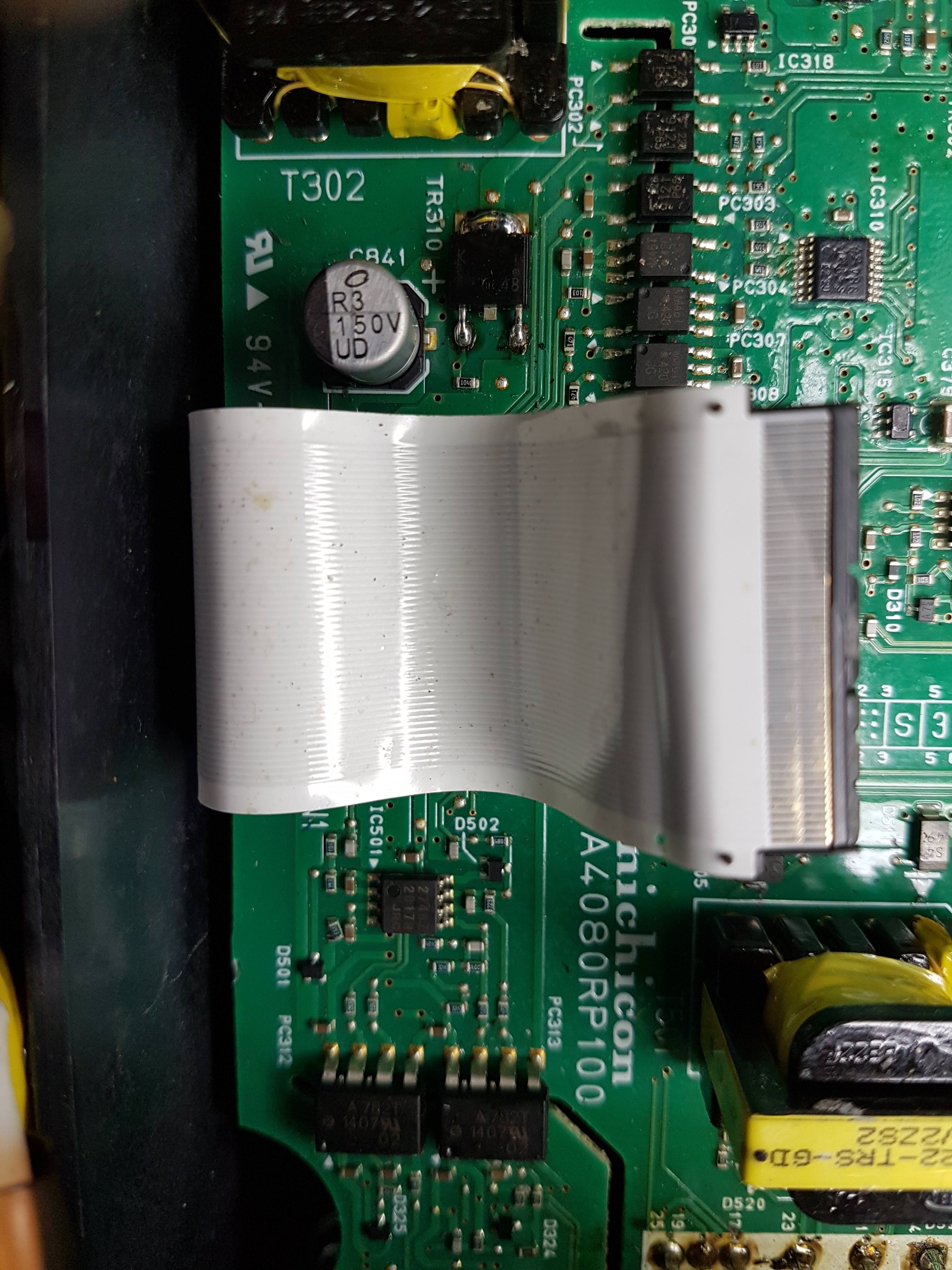
I spotted a resistor that was a bit diagonal and when I checked from the pin of the IC to the VIA I found it was open. one side
was not making contact to the pads. You can see it on the attached photo, between IC501 and D501.
The resistor connects to pin 3 of IC501. It is a 39K resistor. So this would definitely been "A" problem, not sure if it is "The Problem"
or the only problem. Would you have any idea what the function of IC501 is? My meter measured the value as 39.0k the replacement resistor I have put in measures 38.8k I hope this particular resistor is not too critical with tolerance. printed value was 393
First time I've tried to do SMD work in a while, I don't have a SMD Rework setup, so my soldering iron was a bit like cracking a walnut with a sledge hammer. After messing around with it for over an hour including having the bit smaller than a grain of rice flick up into the air and searching for it, finding it and having another go, I finally gave up, and used a thru hold resistors with leads bent soldered to the pads.
Looking at the original part under magnifying glass, it's end caps look good on the top side, but looked like they were not even there on the bottom side where they needed to solder to the pads. So I don't know if this was just not placed and soldered properly during manufacturing, or if it got hot and de-soldered itself and moved diagonally. I'll wait till I get some feedback from you and Coulomb before I try firing it up, so as not to damage anything. (and yes I realise TR310 is a mess with all the excess solder from using it as a test point, haven't got around to cleaning it back up.)


ydd2Ei2.jpg
 
skylogger said:
... was not making contact to the pads. You can see it on the attached photo, between IC501 and D501.
The resistor connects to pin 3 of IC501. It is a 39K resistor.
Well spotted. IC501 seems to be some sort of non-active thing; it doesn't seem to have power supply pins. Unless they're pins 7 and 8, but it doesn't look like it. But they connect to PC312 and PC313, which despite their designations (PC sounds like Photo Coupler to me) are isolation amplifiers. They seem to head off to the output filter section. So I'd guess that they are measuring charger output voltage and current. 39 kΩ is a fairly high value, so it's likely to be in an analog circuit, consistent with the isolation amplifiers.

First time I've tried to do SMD work in a while, I don't have a SMD Rework setup, so my soldering iron was a bit like cracking a walnut with a sledge hammer.
It's usually not too bad with thin solder and a small soldering iron tip. I'm guessing you had a bad resistor, that barely soldered during manufacturing, and came loose with vibration and/or heat in service. You could try soldering it in backwards. The part will cost about one cent to replace, but of course you need to find one, and you might have to buy 100 or more. It's likely an 0603 (1608 metric?) size. You could get 50 of them delivered for AU$0.15 here:

https://au.rs-online.com/web/p/surface-mount-fixed-resistors/2132480/

They will obviously lose a lot of money on just that, (they are the last Australian supplier with free shipping), so it would be nice to order something else at the same time, perhaps some solder wick, or thin lead-free solder, etc.

I'll wait till I get some feedback from you and Coulomb before I try firing it up, so as not to damage anything.
Well, I think it's worth a try, considering that this might be the only problem. I forget now... were your pre-charge resistors burned? If not, I'd say try it out in the car. If those pre-charge resistors were burned, I'd say wait till we can figure out a more gentle test.

Edit: of course, you had the parts on the daughter board blown up. And we now know that these are associated with the charger output. Let's see what Kiev has to say.
 
Back
Top