The Troubleshooting and Repair for On-board Charger (OBC) Thread

Mitsubishi i-MiEV Forum

Help Support Mitsubishi i-MiEV Forum:

This site may earn a commission from merchant affiliate links, including eBay, Amazon, and others.
Hi Jray3, or anyone else willing,
As a backup plan, in case I cannot get the AUS charger I am working on fixed, I am interested in purchasing a 2nd hand one from the USA.
So Far, I've not been able to find any stock in Australia. When I contact 2nd hand sources in USA, Even if I have USA part numbers for the chargers, like 9499D991 and 9499C662, (provided to me by JRAY3 and KIEV earlier) They seem to only want to talk to me if I also supply them with a VIN number for the car. The VIN number for my cars in Australia are no good to use as they cannot look these up in their USA Databases. It seems that I am currently having problems using my Private Messages on this forum. I just tried sending a PM to jray3 and it sits in the OUTBOX, but never goes to the SENT box, so I don't know what needs to happen to get it to move out of the outbox. Also jRAY3, if You have sent me VIN info, I haven't received any PM's in last few days, so maybe the receive is broken too.
I don't know if it violates any rules or privacy, but if someone could post me a USA VIN Number for a 2012 IMIEV , and confirm the part number of the charger used in it, I can use that info as an alternative to source a replacement charger out of the USA if I need to.
 
skylogger said:
Would connecting a transformer with diodes as a test circuit like this drawing, allow to generate signals for the gates to allow testing of the IGBT's
This is not a good idea for a few reasons.
Firstly, I think that 3 VAC (4.2 V peak, about 3.6 V peak after the diodes) is too low. I'm more used to MOSFETs, but I believe that IGBT gates are similar. They usually use 12-15 V square waves with carefully controlled rise and fall times.

Secondly, it has a very non-square wave shape. IGBTs don't like to be in the linear region between saturated and fully cut-off, since they will dissipate much more power in the linear regions.

Lastly, the switching frequency of 50 Hz will be far too low. The transformers will be designed for a switching frequency of at least 10 kHz, possibly around 25 kHz or more. If driven at 50 Hz, the transformer will saturate after a few microseconds, and this will cause its inductance to decrease drastically and the current to increase drastically. This will almost certanly lead to destruction of the IGBTs.

As you mentioned, you'll want to disconnect the existing gate driver circuits if you attempt anything like this. This would be not only to prevent confusion over the results from "interference", but to prevent destruction of the gate drivers as well. These are strong semiconductors, capable of several amps of current into the gates, even if only for less than a microsecond. Driving them the wrong way for up to 20 ms at a time will almost certainly destroy them as well. There may well be series gate resistors on the main PCB that could be removed for this purpose, however.

So: nine out of ten for lateral thinking, and ten out of ten for seeking advice first, but unfortunately this isn't the way to test the IGBTs.
 
skylogger said:
There are common audio transformers quoted as 1K PRI to 8R SEC ratio but they probably don't have the 350-400v rating.
Never connect an audio transformer to mains voltage. They are not designed for this, and would likely saturate at way less than 240 VAC. Saturated transformers look much like a short circuit. Edit: This is in addition to the insulation voltage issue that you mentioned. ]
 
skylogger said:
It seems that I am currently having problems using my Private Messages on this forum. I just tried sending a PM to jray3 and it sits in the OUTBOX, but never goes to the SENT box, so I don't know what needs to happen to get it to move out of the outbox.
This forum uses phpBB software. It's a little unusual in that messages don't move from outbox to sent box until the recipient reads the message. So it's a way of letting the sender know whether or not the message was read.

[ Edit: was received -> was read ]
 
Hi Coulomb:
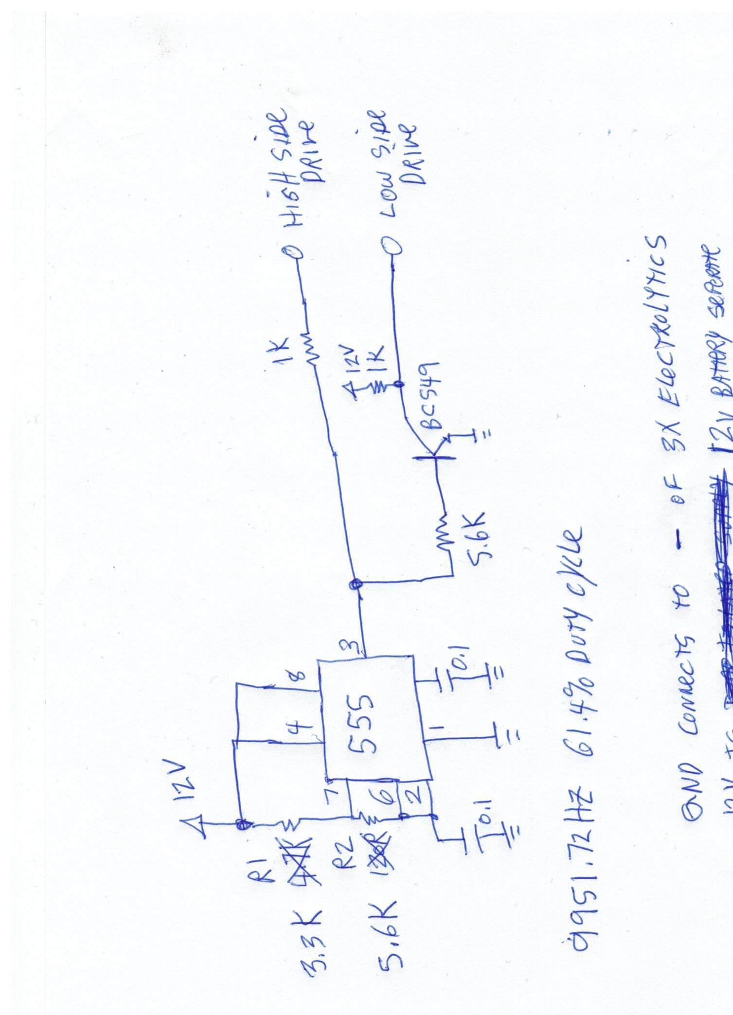
What do you think of using a 555 to generate gate test signals? I've adjusted the resistor values to give a close to 10khz frequency square wave output. The transistor inverts signal so high side and low side get 180 deg switching. This would need help working out what series resistors, and pull ups or pull downs are required for the two outputs:

It sounds like IGBTs are just opposite of transformers, in that you want to apply a square wave to the IGBT so its quickly cut on and off, so you don't waste power in heating up the device, but transformers prefer sign waves for best tranfer between primary to secondary.
quite a bit of difference between this IGBT for this DC to AC, and the Pure sign wave MOSFET Inverters.

q7LVdY8.jpg
 
skylogger said:
What do you think of using a 555 to generate gate test signals? I've adjusted the resistor values to give a close to 10khz frequency square wave output. The transistor inverts signal so high side and low side get 180 deg switching.
Still a few problems.
First, 555s, while strong, may not have sufficient rise and fall slew rates.
Gate series resistors are usually around 22-47 ohms, not 1K.
A 1K pullup is not good; it's far too slow. Outputs need to be push-pull. Really you need a proper gate driver chip.
You also need to isolate the drive for the upper transistor. As soon as it turns on, its emitter goes wildly positive, so to keep it on you will need a gate drive that goes more positive than the emitter. This requires boost diodes. If you don't do this, the gate will go hundreds of volts negative with respect to the emitter, which will surely destroy it.
But finally, and perhaps most importantly, you need guaranteed dead time. IGBTs and MOSFETs take time to turn off; tens of nanoseconds or more. They also take time to fully turn on, but you can't rely on one being slower than the other. So merely inverting the low signal for the high switch isn't good enough.

The dead time is to prevent "shoot through", where the upper and lower transistors are conducting at once, shorting out the power supply. Even if you have a current limited power supply, those 3x680 μF capacitors can pack a lot of energy and blow up the MOSFETs. That's why I prefer to test with a ~50 V current limited supply; the energy in the capacitors (=½CV²) is 64x less with an 8x lower supply voltage. 52 V at the mains terminals turns out to be enough to turn on the power supply for the Elcon chargers. Maybe we can find a similar test voltage for the iMiEV chargers, or find another way to power the control circuit and test with about 12 VDC current limited.

What might work is four 555 timers (say two dual 555 devices). Connect them to trigger off the previous timer's falling edge, with the first one triggered by the last one in a sort of ring oscillator. Initial conditions will be tricky. Arrange the times as say 30 μs, 1 μs, 68 μs, and 1 μs. The two 1 μs timers are for the dead time; they don't connect to gates. The 30 μs and 68 μs outputs connect to say upper and lower gates respectively (only drive one pair for initial testing). So you should get 30 μs high and 68 μs low, representing a 30% pulse width modulation (total period is 30+1+68+1 = 100 μs, or 10 kHz). You'd still need an isolated driver for the upper transistor, so you might as well use a proper gate driver chip. You likely don't have one of those at home, and Jaycar etc likely won't have one you can buy off the shelf.

So the next thing might be to trace the driver circuitry, and find out where they are driven from, and connect their inputs to the four 555 circuit. It's starting to sound pretty complex. You will also need to ensure that the driver chips are powered up.

That might be as simple as supplying 12 VDC or perhaps 14 VDC from a power supply. The power supply for the drivers seems to come from a circuit near the yellow-taped transformer that's on its own. But I don't see how it gets power; it could be 12 V coming through the very fine ribbon cable connecting the top board to the charger board, or more likely from the PFC output (400 V bus). It's likely a high frequency power supply as you'd find in a small plug-pack (wall wart) power supply these days, using the boosted mains voltage rather than merely rectified mains. If so, it depends on the design how low in voltage it will work at. It might be easier to find the outputs of the power supply and supply from a bench power supply, rather than use the power supply in the charger.
 
Howdy sky,

i have some you can try:

JA3215H16CU0 = kiev

JA3215H17CU0 = kiev2

JA3215H13CU025793 = salvage car

JA3215H19CU016564 = salvage

JA3215H1XCU019621 = salvage
 
KIEV: Thanks for all those VIN numbers, with all of these, surely the 2nd hand parts places should find a database match.
are all of those 2012 models or are they different year models?

COULOMB: Looks like creating a test circuit is way harder then I thought. Maybe when the charger is running in the car, CANBUS communications is received which somewhere on the controller PCB is translated to a high/low enable signal for the section that controls the driver timing circuit.
If we can find that, we can force it high or low similar to the jumpers on the other chargers that you have worked on previously.

Another idea would be to use the testing transformer idea I first posted, but with a 24v center tap, so you get 2x 12v signals, and then put each of these half wave signals to a Triac, Like motor speed controllers use. This would allow fire the triac when it reached a trigger set point. This chopping would also create the dead time gap needed to make sure the High and Low sides are switched off completely before the next cycle.
You would end up with a chopped 12v square wave but still some round at the top.
 
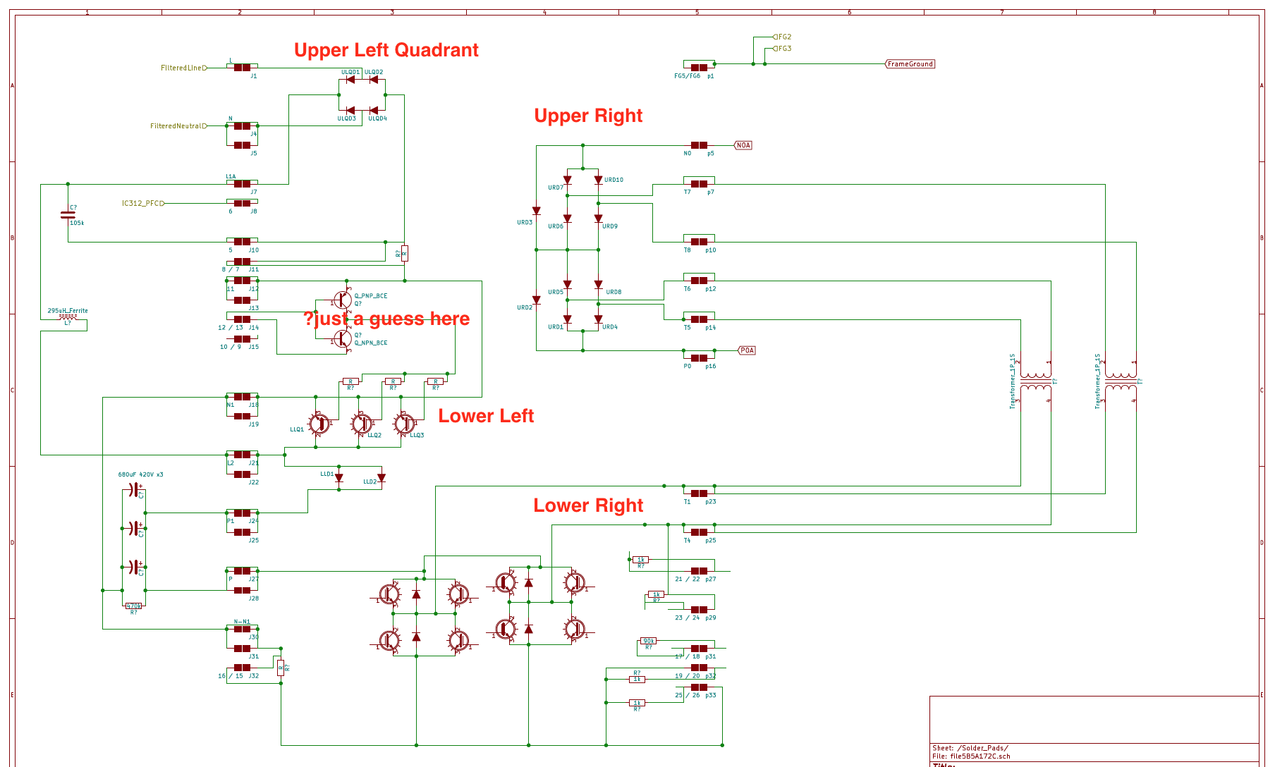
i tried to correct and add components seen in the x-cavation. i numbered the semiconductors starting from left to right by their physical location in each quadrant.

It looks like a push-pull drive circuit for the PFC "FETs" in the lower left quad, but this is just a crude guess since we don't really know what is under there. i think the positive drive voltage come in thru pin 13, so maybe that could be checked to see what is present on that pin. pin 12 might be the drive signal from the PFC control chip, IC312, TI UC2854, which does have a 1A push-pull output.

There appears to be a couple of current sense resistors, so they were added but the values are unknown.

From your in-car testing, and the current measurement, it seems as if the AC input relay is not being commanded, or it is bad.

Be careful with the testing, it will be very difficult to replace or repair semiconductor parts on the waffle plate. Let me know what is highest priority and i'll focus on that aspect of tracing.

8xWaPaN.png
 
kiev said:
i tried to correct and add components seen in the x-cavation.
Ah. In my post, I meant X-cavation to mean the eXacto knife process, but it can stand for the X-ray photos as well I guess.

It looks like a push-pull drive circuit for the PFC "FETs" in the lower left quad, but this is just a crude guess since we don't really know what is under there.
Good guess I think. I had noticed that area and not figured out what it could be.

i think the positive drive voltage come in thru pin 13, so maybe that could be checked to see what is present on that pin.
I think you are right, but have the NPN and PNP driver transistors reversed. Yes, it would be good to know that the voltage is on pin 13 with respect to pin 11.

pin 12 might be the drive signal from the PFC control chip, IC312, TI UC2854, which does have a 1A push-pull output.
Great to know. So it would also be good to know if there are pulses on pin 12 with respect to pin 11 (using dual trace and diff).

There appears to be a couple of current sense resistors, so they were added but the values are unknown.
Brilliant! I was thinking that these were capacitors, and could not make sense of the thin wires. Every PFC circuit needs to measure current, so the mains current will stay in phase with the mains voltage for near-unity power factor. This will be the feedback. It's in the negative leg of the power circuit, for ease of measurement. So I believe that your shorting of pins 8 and 7 is incorrect, it will be the shunt resistors (two in series). To measure it, I'd apply 1-5 A from a current limited lab power supply to pins 5 and 11, and measure the voltage drop with a multimeter, probably on the millivolt scale. Then just use Ohm's law R = V/I. They provide the Kelvin connections to make this accurate.

From your in-car testing, and the current measurement, it seems as if the AC input relay is not being commanded, or it is bad.
I was still thinking that the low voltage measured could be across the inductor, but thinking about this more, I tend to agree with you now. There is no significant current being drawn, apart from narrow pulses to charge the capacitors, and whatever voltage there is across the unknown impedance it will still scale with mains current. There will at least 100x as much current at full load, and you can't have ~150 V (1.57 x 100) dropped across that impedance. So this must be the pre-charge resistors, and the input relay must be unenergised, or its contacts open circuit.

So @Skylogger, you need to make sure you don't cause any significant power to be drawn until that issue is settled. Your pre-charge resistors apear to be intact at this point, but they won't stay that way if you start charging the pack for real with the input relay turned off.

Thanks as always Kiev for your thoughts.
 
kiev said:
Let me know what is highest priority and i'll focus on that aspect of tracing.
You probably mean people that are actively attempting to repair their charger, like Skylogger, but my thought is to start with the power supply for the charger board. That would be the corner with the yellow-taped transformer (or multi-winding inductor) on its own. The pair of transformers with "GD" in the part number are probably Gate Drivers.

After that, I think perhaps the PFC circuit. It would be nice to know if there is an enable signal for that, which is preventing the PFC stage from boosting Skylogger's mains beyond peak mains voltage.

Just my suggestions.
 
@coulomb, good eye to catch my drawing mistakes. i was tired, it was late and i was in a hurry to get that done so i could post it up. i saw the errors after i had already printed to file. Between rotate, mirror horizontal and mirror vertical i should be able to get the parts drawn in a decent manner...

i noticed some blistering in Jay's unit in the AC input doghouse potting at the end of the coil toward the side of the box--i will go ahead and dig all of that mess out just to see if there are other components (not likely) and if the end of the coil is damaged or heat-affected. Then i'll get after the low-voltage power supply and PFC traces.

That flat ribbon cable from the top board to CN1 on the bottom board has 50 pins at 0.5mm spacing--i'm having a hard time seeing even with a magnifying glass...
 
Having trouble finding data sheets on some of the devices related to the low-voltage power supply.

1. photocoupler used 7 times across the slot cut in the board to isolate the CN1 connector. It is a 4-pin SMD opto device with a Toshiba logo but the part number, 9121, seems to be not a standard part.

2. IC314 and 317, a 6-pin (5 + tab) smd part marked, M05 0KU, some sort of voltage regulator on the output of the transformer
[edit: this is a NCP4641 5.0 volt regulator by ON Semi, package is sot-89-5-1 (pin 2 and tab are connected)]

3. Three Diodes marked, 2U 1D.

4. IC702, an 8-pin smd from JRC, Japan Radio Corp, but part number partially etched, 2x69x T008H JRC.
[edit: found it, 2369Z, a flyback switching regulator chip.]

5.
 
There is a DC supply voltage coming from the Top Board across the CN1 connector on pins 5-8, with ground on 1-4 and 47-50. This is filtered by an electrolytic cap, C841, 15uF 35V, and is then chopped thru a transistor TR310, an N-FET 2SK3484 100V 16A, to excite the primary on pins 8-9 of the CV transformer, T302. The gate is driven by a 10W flyback switching regulator chip, IC702 JRC 2369Z.

There is a First secondary on T302 pins 6-7 that is half-waved thru diode D334, 2U 1D, that ties back to the CN1 supply ground and regulated by IC317, M050 5V regulator. This 5vdc is used for the supply voltage on two isolation amplifiers, PC312, 313, Broadcom A 7827. PC313 is sending the output current sensed thru R232, 0.008 Ohms, across the isolation slot to an op amp, and then on to the CN1 connector back to the top board. PC312 is sensing the [edit] HV output voltage and sending it back up to the top board on CN1, pin 42. So the box is smart enough to measure itself and likely won't come on if something doesn't feed back properly to the top board.

There is a Second secondary winding on pins 2-3 that is half-waved thru D328 2U 1D, filtered by C367 10uF 25V, regulated thru IC314, M050, that creates another 5vdc routed to IC301, etched part number
?277?.

And there is a Third secondary winding on pins 2-4 is half-waved thru D331, filtered by C 845 15uF 35V, that provides ~ 16.6 vdc supply voltage for the PFC chip, IC312 UC2854 and to the solder pad pin “13”, which is the positive rail of the push-pull gate driver for the 3 PFC gates. There appears to be an adjustable shunt regulator at IC318, marked TACQ, TI TL431-Q1, that provides a feedback signal back to the flyback regulator chip, IC702, that is pulsing the transformer. The 16.6 was my calculated value based upon the resistor network for the shunt regulator.

The ground reference for the 2nd and 3rd secondaries is to solder pad “11”.

So if possible check the top board to see if it is generating the initial DC voltage from which the low-voltage supplies on the bottom board are created. i don’t have that board in front of me right now, but it would be a somewhat easy fix if the issue were the low-voltage supply on the top board—without that supply the bottom board would not function.

The 5V drive for the AC Input Relay coil comes down from the top board on CN1 pins 26-29 and the return is pin 25. If this were defective then the relay couldn't come on. You might look for one of those M050 5vdc regulator chips in the vicinity as a source for the coil voltage.
 
Hi Kiev:

It's amazing your tracing across the fine pitch 50 way connector. I've run a few test so far, at a snails pace, disconnecting the top board, standing it up vertically so i could solder wires to the pins on the two white strips, that run to a block of screw terminals, then put it all back together, connect AC, and do measurements across the terminals. It's a bit of a worry trying to lift the top board up and down over and over without damaging the flex strip.

I just got through soldering some wires to pin 3 and the Tab on Transistor T310, and after supplying AC, I've found this first rail to be dead.
Do you think this first rail should be active, even with the communicatitions connector not plugged in (box still on bench not in car)
In your previous message, you say what the voltages should be for all the supplies that get created from this first rail, but I did not see where you mentioned what this first rail voltage actually should be.
The communication cable that connects to the TOP PCB, Via connector E-02 on the maintenance manual schematics, has a PIN 7 RED wire that connects back to the 12v battery. There is also a PIN 2 VIOLET wire that connects to 12v via the contacts of the On board charger relay.
These both reference to PIN 10 Ground on this E-02 Connector. I am thinking that the main rail coming across the flex cable will probably be dead until 12v is supplied to pins 2 and 7 and ground connected to pin 10 of E-02.
There is also a PIN 12 Beige colour wire on this connector that is a signal called CHGP from the EV-ECU, That may have to be at a particular voltage to enable the charger.

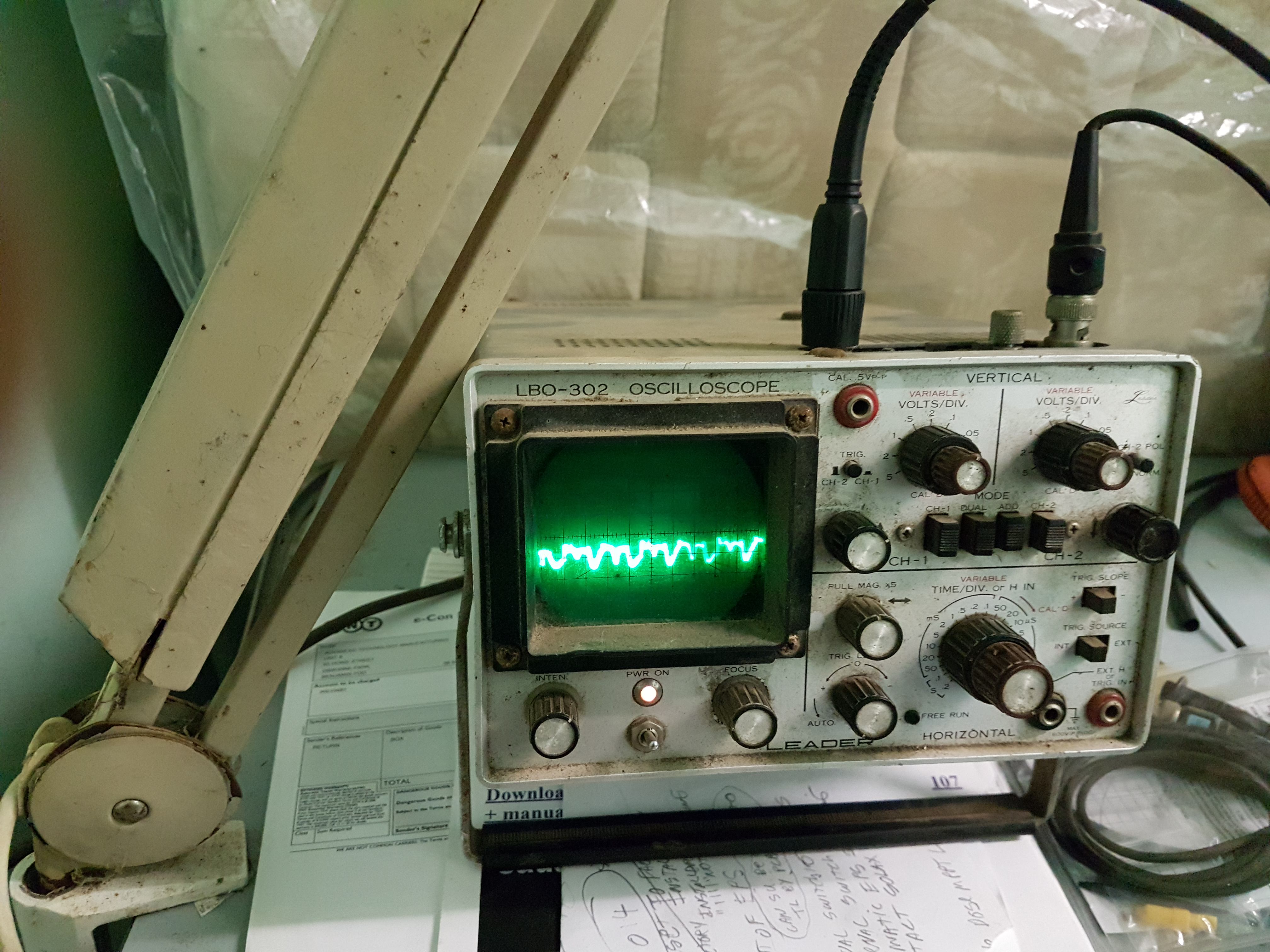
I also connected my old half dead 50 year old oscilloscope in dual chanel diff mode to see what is across pin 11 and 12. attached is what I see, but its probably just noise from the fluro lights i'm working under. looks like 4vp-p

lvAtY9d.jpg
 
skylogger said:
Do you think this first rail should be active, even with the communicatitions connector not plugged in (box still on bench not in car)
It looks to me like the power is coming through the comms connector. The mains conditioning seems to be for the two terminals that go to the charger board. So that would be a provisional "probably no".

In your previous message, you say what the voltages should be for all the supplies that get created from this first rail, but I did not see where you mentioned what this first rail voltage actually should be.
Nearly half of the top of the top board seems to be devoted to a power supply; there are a lot of inductors, electrolytic capacitors, and power semiconductors underneath.

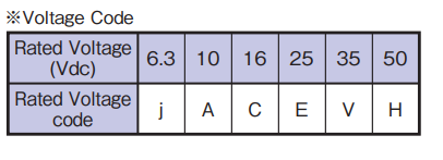
I see at least two capacitors with the "V" voltage code (220V and 330V). These are too small to be 220 volts and certainly not 330 volts.

dc0918e1aed1d899c8328e2acc1b604384ecc4f5.png


From https://forum.digikey.com/t/smt-electrolytic-capacitor-with-no-voltage-rating/974 .

[ Edit: so these would be 220 μF and 330 μF, both at 35 V. Other capacitors there are rated at 470 μF and 10 V. ]

A 35 V rating suggests 24 V nominal design voltage. The next lowest code is E for 25 V, too close for comfort. The battery voltage, nominally 12 V, is a little low for sending over thin wires, and besides it varies from 11 to 14.4 V depending on the state of charge of the battery, and the loads.

[ Edit: besides, a lot of industrial gear seems to like 24 V. ]
[ Edit: so what I'm trying to say is, I suspect that there will be a regulated 24 V sent from the top board to the charger board. ]

I am thinking that the main rail coming across the flex cable will probably be dead until 12v is supplied to pins 2 and 7 and ground connected to pin 10 of E-02.
Yes, that seems to be the case.

I also connected my old half dead 50 year old oscilloscope in dual chanel diff mode to see what is across pin 11 and 12. attached is what I see, but its probably just noise from the fluro lights i'm working under. looks like 4vp-p
Difficult to tell, but not even 4 V peak to peak is certainly too low.

[ Edit: had capacitor values wrong. ]
 
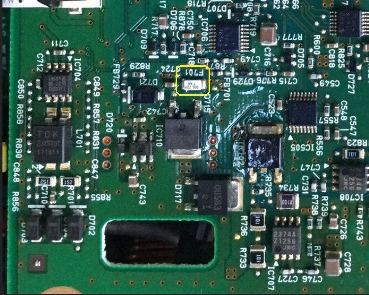
i found a surface mount fuse F701 on bottom of the top board near D715. The fuse is fed from CN101[ pin 12], which is likely 12V power into the control board. This is in-line with the power supply to the bottom board pins 5-8

Will post photo later, but it would be easy to check--hopefully that fuse is blown and it will be an easy repair.
 
kiev said:
i found a surface mount fuse F701 on bottom of the top board near D715. ...
Will post photo later...
I can save you the trouble. Well spotted!

emKQwRh.jpg


Now to figure out its specifications. Something like 2410 imperial [ edit: was 1608 ], 72 V, wild guessing about half to one amp? Soldering in a 20x5 1 A fuse could make for a very temporary fix. Or perhaps soldering in a 20x5 fuse holder; soldering fuses often seems to ruin them. Insulate well, of course.

[ Edit: Seems there is no such imperial size as 1608. I was perhaps confusing with metric sizes. ]
[ Edit: My guesses were pretty bad. Kiev says it's an imperial 1206 size, and 4 amps. ]
 
That's the one--it is marked SOC 72V T 4A on my board. i hope the fuse did it's job and blew due to inrush current into C702 and C701, the big cans on the top side of the top board.
https://www.ebay.com/i/172933474295?chn=ps

http://socfuse.com/products/index.html

i didn't think to ring out the control cable from the exterior 13-terminal E-03 connector, to the interior CN101 12-terminal connector, [pin 12] is the one that supplies the bottom board--if that fuse is blown then the charger won't work.

Looking at the charger control wiring diagram, there are 2 12V feeds into the OBC, one may be always connected thru a fusible link E-03p7, and the other E-03p2 is switched thru a relay controlled by the EV-ECU.
http://mmc-manuals.ru/manuals/i-miev/online/Service_Manual/img/90/HBT04E01AF00ENG.pdf

http://mmc-manuals.ru/manuals/i-miev/online/Service_Manual/img/90/HBT04E01BC00ENG.pdf

http://mmc-manuals.ru/manuals/i-miev/online/Service_Manual/img/90/HBT04E01CC00ENG.pdf

http://mmc-manuals.ru/manuals/i-miev/online/Service_Manual/2012/index_M1.htm
 
kiev said:
Looking at the charger control wiring diagram...

http://mmc-manuals.ru/manuals/i-miev/online/Service_Manual/img/90/HBT04E01AF00ENG.pdf
I don't see any CAN connections to the charger. It seems to only have the CHGP input, the pilot signal (pin 3 of the J1772 charge port), and the switched 12 V input. It looks like the EVCU just says yes or no to "charge as much as the pilot signal tells you, till the battery is full". Maybe the CHGP is for charge partial, and go/no-go is all via the 12 V charger relay.

There may still be charger enable CAN messages, but handled by the EVCU, which result in changing the EVCU's outputs CHGB and CHGP. That might mean that if these chargers prove to be hopeless to repair (I don't think so, but they might turn out that way), then replacement with a more generic charger may be possible.
 
Back
Top