The Troubleshooting and Repair for On-board Charger (OBC) Thread

Mitsubishi i-MiEV Forum

Help Support Mitsubishi i-MiEV Forum:

This site may earn a commission from merchant affiliate links, including eBay, Amazon, and others.
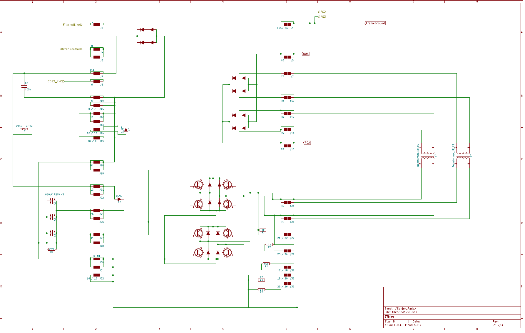
Here are my tracing notes on the two solder rails, left and right, of the bottom board. My plan is to replace all this mess with a pretty schematic drawing using Kicad. i didn't find a round solder pad or via in the components list, so i used these square solder pads on the rough draft drawing and labeled them with what is printed on the board. i've numbered them from 1-32 and 1-33 for my convenience as if they were connector pins. The designation top and bottom refers to components on the board or below it on the waffle plate. BT is the blade terminals soldered to the board for connecting to the magnetics.
Qpwzj7y.jpg


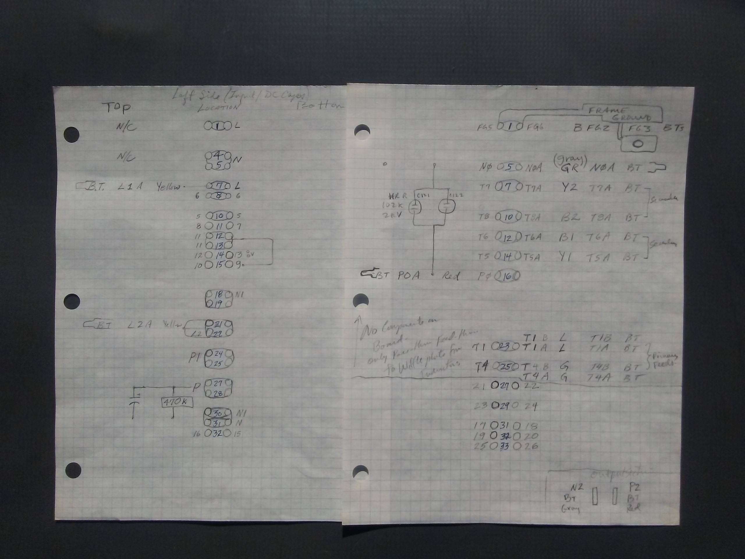
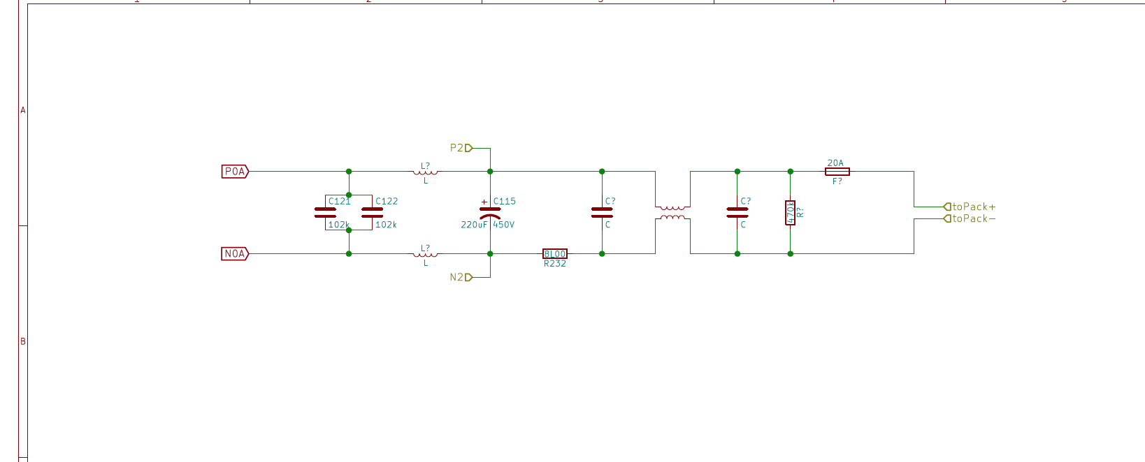
Here are some measurements of the inductor characteristics and a sketch of the final output filter before it leaves the box on it's way to the battery pack. These are marked as "zebra" transformers but i couldn't find any data sheet or info about these part numbers on their website.
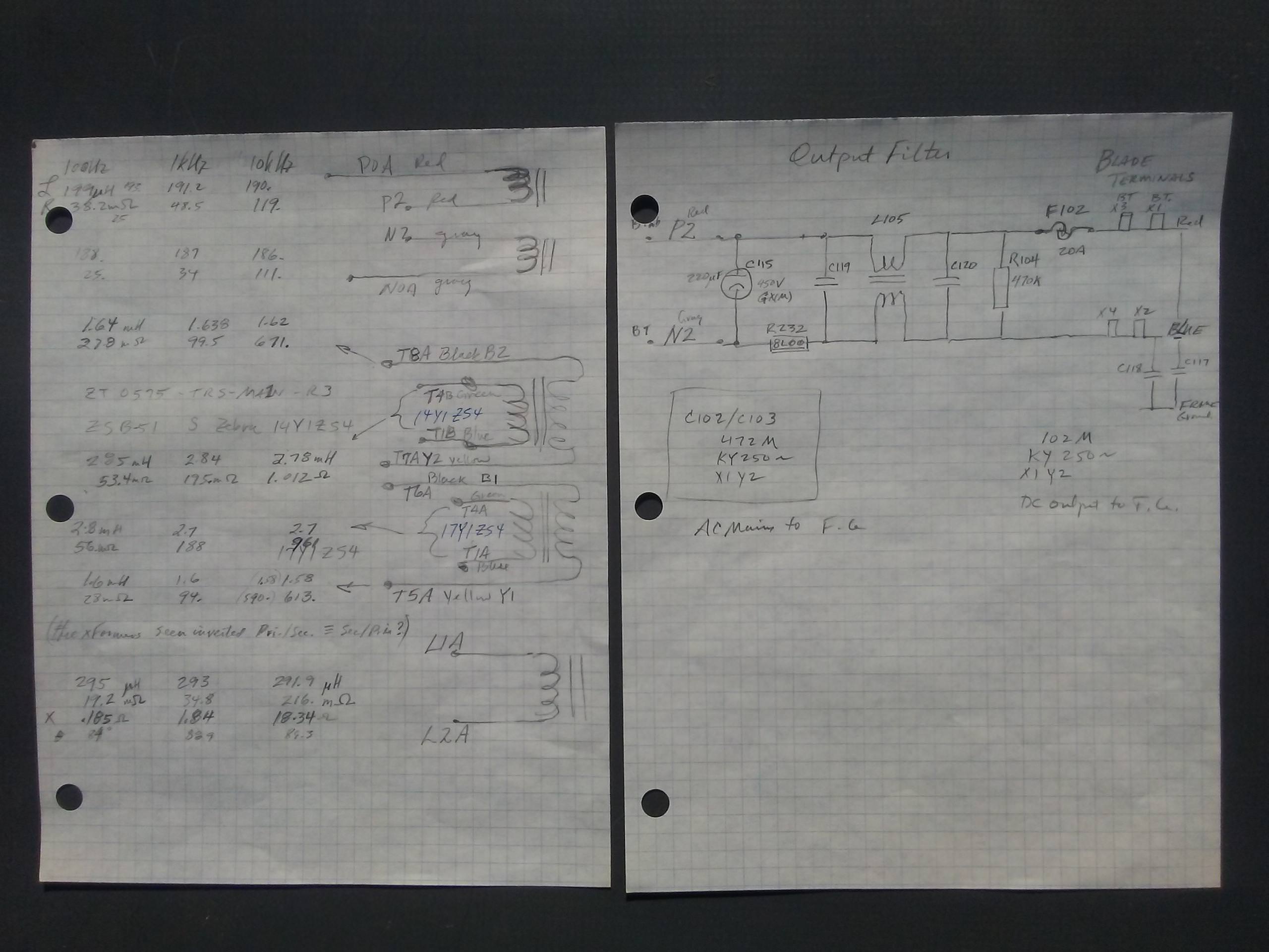
PM95O7F.jpg


Rough draft Kicad sketch with measurement notes from the waffle plate (rectifier diode and FET diode drops). Toward the top center is a dashed box labelled Top with 2 capacitors--those are the output filter snubber caps blown in Jay and sky's potted doghouse.
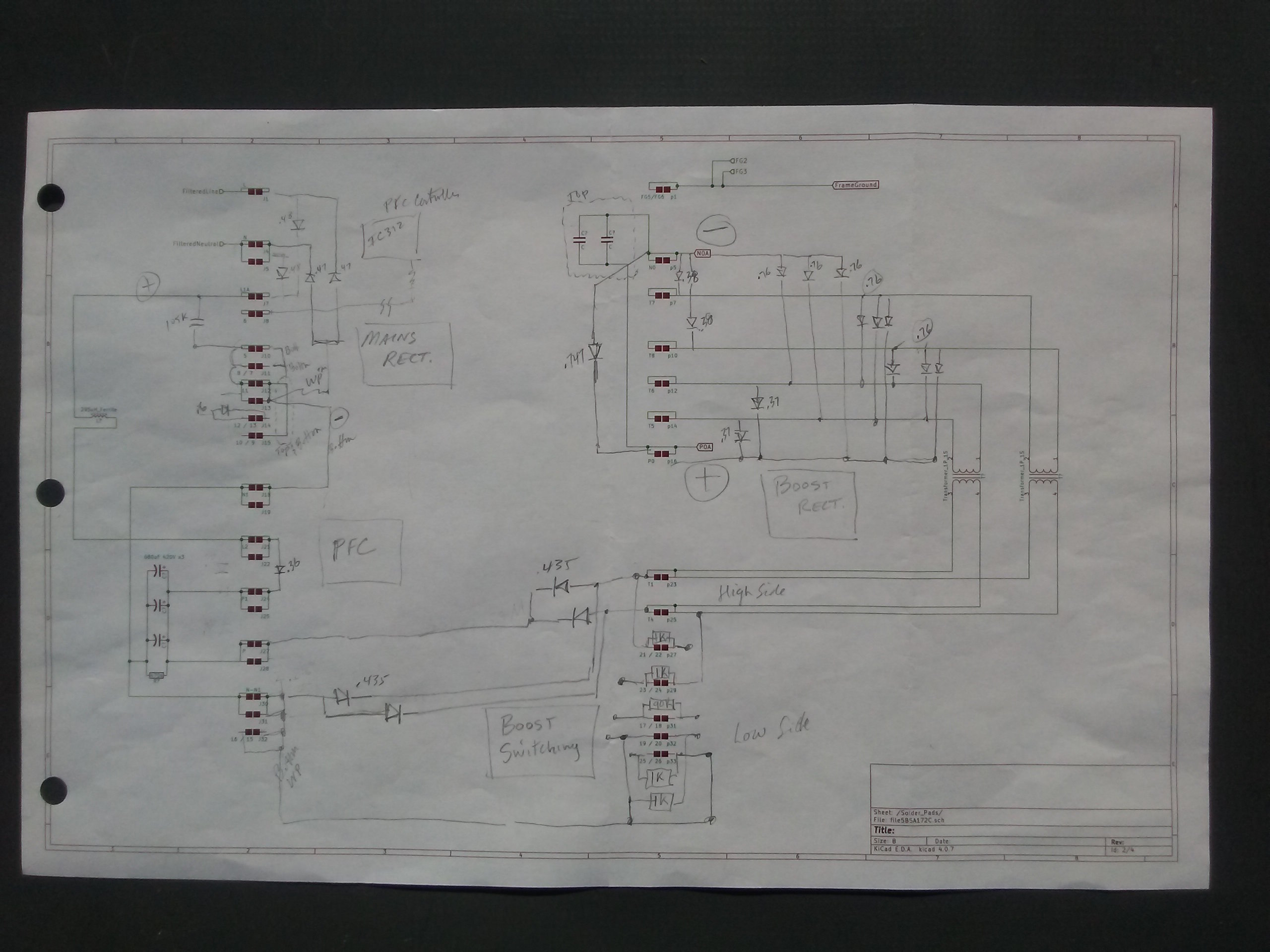
VbRyfIb.jpg


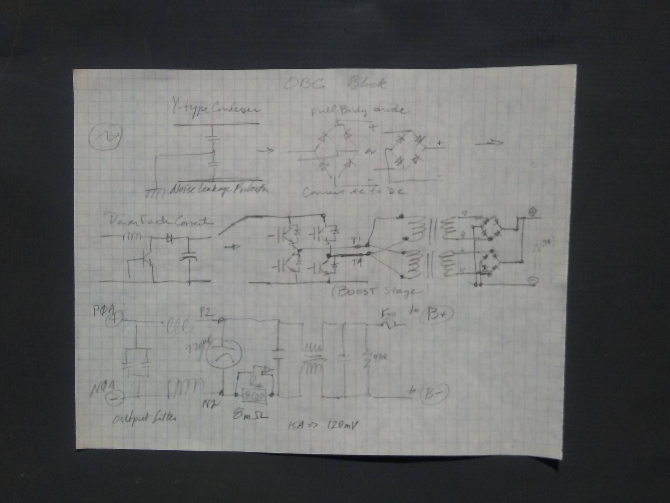
Here is a sketch of all the easy stuff i've traced that matches up with the OBC block diagram that Mits put in the technical information manual. This is the high-power analog stuff that carries the beans. The low level digital logic and control will need to be traced to tie it all together--but it can be more difficult and time-consuming to figure out due to the microscopic size of the components...
5MiigDL.jpg


.cheers,
 
Hi Kiev:
That is the most awsome reverse engineering I've seen. At the moment, I put the faulty charger back in my friends car, so they could still use the DC-DC Converter section to charge the 12v battery, and can use a Chademo quick charger to keep the car up and running.
I have access to a wrecked IMIEV that is also a 2010, but the part number on the working charger inside it is different, and the inside
PCBs are totally different. I think the Wrecked IMIEV was a beginning of year 2010 model, and my friends IMIEV is End of Year 2010 model.
I had put the project on hold for a week, because I ran some test with MUT III. I could look at Hardware and Software revisions on BMU, CMU, MMU, But the MUT III would not communicate with the OBC. I only just tried this on two other working IMIEVs and have the same problem, so it looks like my problem with communications between MUT III and OBC are with the MUT III and not really a fault with the OBC. I'm using a MUT III Clone from china, and the MUT III Second Edition software that I acquired from Russia. I think the MUT III talks to all the ECUs on the same CANBUS, but the CANBUS That connects to the Diagnostic socket on the car is a different bus than what connects to the OBC.
So now that I know that the communications problem was a red herring, Tomorrow, I plan to swap chargers, so my friend will have a known good charger put into there car (although older revision), to see if there are any other faults in the car. This will allow me to take the faulty charger from his car, and use the wrecked IMIEV that I have access to as a test bed. I'll do a quick test of soldering wires to the points that you gave me on the output of the doghouse and check the voltage there so I can confirm if the first section of the block diagram is working.

I used to play a bit with the older desktop PC's, and I think I remember that you never power up the ATX Switching power supply without it being plugged into the mother board, or a dummy load, or the power supply would blow up. I was wondering if this IMIEV Charger and DC-DC Converter might be simular. Do you think if AC is applied to the AC input of the charger section, but no loads applied to the 12vdc output or the HV 360VDC output, would this possibly damage anything. Also, if there is no load on the 360vdc output, do you think the charger could be tested for short periods of time without coolant running through it, like testing it on a bench instead of fitting back in the car?

Besides the AC, 12V, 360V Connectors going to the box, there is the 4th connector that allows the charger to communicate with the rest of the car. I would assume there are pins in this connector that have to be grounded or 12v applied, or some CANBUS communications required for the Charger or DC-DC Converter to be active. Would you have any info on what would be required at this connector to be dummied out so as to be able to have the Charger in enabled mode. I can then test voltages at the outputs of each block in the block diagram and see what sections are still working and which are dead fairly quickly?

Thanks again for all the great documentation and work you are doing, With your help, I might be able to bring live back into this charger.
 
kiev said:
Here are my tracing notes on the two solder rails, left and right, of the bottom board.
Great work; thanks for starting this! :cool:

Rough draft Kicad sketch with measurement notes from the waffle plate (rectifier diode and FET diode drops).
I think that most if not all of your 0.7 V+ diodes are phantoms; other ~0.37 V diodes in series joined by low resistance windings. I get that this is just rough notes; may as well record all the readings, and make sense of it later.

I see no IGBTs here, but my guess is that they're in the lower right quadrant, with the 1K resistors being gate pull-down resistors perhaps. There are 8 squares there; my guess is that these are IGBTs (the type without integral diodes) and the back diodes right next to the collector and emitter connections.

The other thing that occurred to me is that maybe there are two sets of full-bridge IGBTs (the more common type with on-die back diodes), each driving their transformer primaries separately. But I can't reconcile that with your tracing.

Toward the top center is a dashed box labelled Top with 2 capacitors--those are the output filter snubber caps blown in Jay and sky's potted doghouse.
Ah! So these are in fact across the DC output. I'm not immediately seeing a reason for these to blow.
 
skylogger said:
I used to play a bit with the older desktop PC's, and I think I remember that you never power up the ATX Switching power supply without it being plugged into the mother board, or a dummy load, or the power supply would blow up. I was wondering if this IMIEV Charger and DC-DC Converter might be simular.
I don't believe so. I operated a lot of older Elcon/TC chargers on the bench with no load and had no problems. Of course, the iMiEV chargers could be different, but my gut feeling is no. Switching the DC-DC (12 V charger) with no load might be a different story, but I'm pretty certain that merely applying power and no CAN signals, no switching will happen, and no damage will be done. Applying a small 12 V battery for charging on the bench is a lot easier and safer than a 360 VDC battery.

Also, if there is no load on the 360vdc output, do you think the charger could be tested for short periods of time without coolant running through it, like testing it on a bench instead of fitting back in the car?
Again, I did this all the time on the Elcon/TC chargers. I'd say the iMiEV chargers would be fine on the bench with no cooling.

I'm a great fan of running these chargers initially at least from a current limited power supply. [ Edit: Into the mains input. The DC-DC might similarly work with much lower voltage at the 360 V input. ] I settled on 52 V (two 26 V 3 A power supplies in series) for the Elcon/TC chargers. This was enough to get the power supply chip working, and if enabled, the PFC stage could boost the 52 V (more like 50 V after the input rectifier) to the ~385 V that the power stage wanted. There were in fact jumpers (really just pairs of pads labelled something like J8) that could be used to first switch the output stage at 50 V, then if that worked, switch at 385 V (some 64x the energy in the bus capacitors with 8 times the voltage). There was even a jumper to cause the output stage to switch even though the microcontroller wasn't yet commanding output, and it wasn't seeing a battery to charge. This would put some 120% of maximum voltage at the output if all was working. By working methodically through the procedure, you'd be able to test the power stages with gradually increasing power levels, minimising the chances of having things blow up on the bench. I would never apply mains power till the charger was back together (apart from the cover with 28 screws), so the 400 V parts were safely tucked away, and the MOSFETs had their heatsink clips on. These Elcon/TC chargers were only air cooled.

[ Edit: heatsinks on -> heatsink clips on ]
[ Edit: 120% of rated -> 120% of maximum ]
 
coulomb said:
...

I see no IGBTs here, but my guess is that they're in the lower right quadrant, with the 1K resistors being gate pull-down resistors perhaps. There are 8 squares there; my guess is that these are IGBTs (the type without integral diodes) and the back diodes right next to the collector and emitter connections.

The other thing that occurred to me is that maybe there are two sets of full-bridge IGBTs (the more common type with on-die back diodes), each driving their transformer primaries separately. But I can't reconcile that with your tracing.

That is what i was thinking also even though i didn't draw it up that way in the block diagram, but it seems likely since there are 2 separate Boost transformers that there are 2 separate H-bridges in parallel.

Looking at the waffle plate, i think the AC bridge rectifier is in the upper left quadrant, the PFC switches and blocking diode are in the lower left, the Boost H-bridges are in the lower right, and the Boost bridge rectifiers are in the upper right.

i too am trying to figure out how to test a charger on the bench.
 
I have noticed in the past how warm the interior of my car gets while charging on L2 (I'd say about 90 degrees with the windows up) so I started using my home DIY upgraded Mitsubishi evse that someone posted about here last year where you change out a small power supply and the cord plug and and it works on 240 VAC. The only problem with the diy upgrade is without programming it charges at around 1800 watts. I assume that it's still programmed for 8 amps but since now it's running on 240 V, it's now working at twice the wattage. It's more like a L1 evse.

The interior now feels much cooler and yesterday I opened up the engine hatch to check the charger temperature and found it to be very cool, maybe 90 degrees to the touch. That was after about 2 hours of charging on an 80 degree afternoon. I'll find my ir temperature gun and take some temperatures this evening to be more accurate. I've been doing this with a time clock for about a year now. Ed
 
skylogger said:
I have access to a wrecked IMIEV that is also a 2010, but the part number on the working charger inside it is different, and the inside
PCBs are totally different. I think the Wrecked IMIEV was a beginning of year 2010 model, and my friends IMIEV is End of Year 2010 model.
The junkyard charger that I replaced my failed unit with also had a very different model number, though it looked identical on the outside and under the lid. Original on my May 2012 car was labeled as follows
9499D991
Serial.00692 V100
ZHTP1529R 2012.04.20
nichion
bar code= DPT1529ABR00692V100

The replacement came from an older car with far fewer miles
9499C662 NAS
Serial. 00497 V101
ZHTP1546R 2011.11.01
nichion
bar code= DPT1546NAS00497V101

We also know there are at least two different versions of the charger internals for our cars that work, so assuming the battery was of the same capacity (16, not 12 kwh) and using the same cells, I'd say to trust your common sense more than the sticker on the charger and try that swap if it looks like a match...
 
Here is a cleaned up drawing with what i think may be on the waffle plate, being shown in the central region between the two solder pad strips. The IGBTs are just a guess since the part numbers have been etched off the chips (in addition to being covered in epoxy). There is a small label on the side of the waffle plate with a separate part number, CZ1525RPWR012 2R04 No. 0044.

rEe2W1r.png


Output Filter

qsMS9DD.png
 
Hi Kiev:
You've really made life a lot easier with all the documentation you've done for these chargers.
I've got the charger out of the can, on the test bench, and using a power cord with fuse from wall
socket to the AC input ring terminal screws on the top pcb.

I tested the ACTIVE and NEUTRAL test points you showed me on the white strips of pins from the waffle.
The output from the Doghouse is measuring 239vac which is same as the wall outlet (here in australia)
so that looks like all is good with the doghouse.

I've used your new cleaned up schematic to check output of the rectifier bridge, and I measure 247vdc there.
I've check the voltage across the three BIG electrolytic caps, and there is no voltage there. This makes me think
maybe the Diode D7 is blow open. It's a bit slow going, as I have to disconnect all the connections to the top PCB,
Do a solder connection to test points, then put top pcb back on and run a test.
i'll test Diode D7 with an ohm meter once I get a chance to get to it again.

If this diode is blown open, I guess the next step is working out what part number the diode would be.
Depending on how many other parts are bad in the waffle board, I was thinking of maybe getting a replacement diode
that could be heat sinked to the case somewhere else, and run wire from it over to the the pads on the white strip.
Sort of a bypass operation ranther than removing the waffle board, cutting through the epoxy and replacing the original part.
Not the sexiest way of doing it but might get it working that way. (This would only work for parts blown open not shorted)
 
Howdy sky logger,

i think the diodes are labelled D? as i didn't have any reference designators visible for the components on the waffle plate. But you are probably referring to the diode between L2 and P1 on the left hand solder strip, as that is in the circuit path from the rectifier thru the big inductor (bottom right corner of box) and then on to the big electrolytic cap bank.

i'm not sure why the DC is only reading 247--i would expect to see ~340vdc with 239vac mains.

do you have anyway to measure the mains current into the box while you are making the voltage measurement?

i think the diode(s) you are chasing are in the lower left quadrant of the waffle plate.
 
kiev said:
i'm not sure why the DC is only reading 247--i would expect to see ~340vdc with 239vac mains.
Because it's pulsing DC with no significant smoothing capacitors to keep the voltage near the peaks. If that PFC diode was working, we'd see the ~340 VDC at the 3 large capacitors (but still ~247 VDC at the bridge output). The exact reading depends on whether the meter is true RMS reading or average reading, and how much smoothing is happening due to small capacitances here and there. Particularly the 105 (1 μF) between pins 5 and L1A.

Everything is pointing to an open circuit PFC diode at this point.

I like @skylogger's idea of bypassing open circuit components. It may even be possible to bypass some shorted components by judicious cutting of the headers coming off the waffle plate™.

[ Edit: bypass some shorted components. ]
 
I'm using a pretty cheap volt meter that is probably way out of calibration, so that would affect my measurements also.
I've soldered four wires to a terminal strip, 2 wires from across the 3x BIG electrolytics caps, and 2 wires going out to the
transformers. On the Ohm meter readings (in diode testing mode) when I go across the combinations of these 4 points,
I see readings of 0.8xx one way and Infinity the other which is what would be expected reading across two diodes in series
that are across the IGBT or MOSFET or what ever it is. So to me, I don't see any shorts or opens across the power devices.
When I first apply AC at the Input, The voltage across the Electrolytics measure 348vdc but then after a 10 seconds, I start
seeing this start counting slowly down. I don't leave the AC applied for more than a minute, as this might be a sign that
something is warming up. I've got an old 50 year old oscilloscope I might try and fire up, and see if I can see any oscillating
signals going to the pads around the 1k gate pull down resistors. I've got to rig up an isolation transformer to power the oscilloscope,
because its earth lead would flow back through hose wiring back to Neutral (back at the meter box) and cause problems.
I suspect that there are no gate signals to cause the power devices to switch. This might be due to drivers being damaged, or may just
be due to it not being in the car and not having the communications cable pluged in to enable running of the charger.

I did notice that when this Charger was fitted in the car, and I plugged in the AC Cord to the car, The charging light on the dash would
come on and blink a few seconds and then the yellow triangle with the ! would appear and charging would shut down.
To me this means the charger was at least telling the rest of the car that AC power was being applied to the charger.
 
skylogger said:
I'm using a pretty cheap volt meter that is probably way out of calibration, so that would affect my measurements also.
I get nervous when people use cheap multimeters on gear with 400 VDC. Might I suggest at least a CAT II model from Jaycar or similar for maybe AU$50?

So to me, I don't see any shorts or opens across the power devices.
I'm not convinced yet that you have checked the PFC MOSFET/IGBT and diode. The back diode for the PFC MOSFET/IGBT should read around 0.4 V, not around 0.8 V.

When I first apply AC at the Input, The voltage across the Electrolytics measure 348vdc but then after a 10 seconds, I start
seeing this start counting slowly down. I don't leave the AC applied for more than a minute...
I can appreciate that. But how far does it sag in that minute? Only to say 340 V, or way under 300 V?

It's starting to sound like either the PFC diode or inductor are intermittently open circuit. Ah. Or the input relay is disconnecting, and the 4.7 Ω resistors across the input relay are open circuit. Is it possible to hear the relay operate, or is it too hard to get to, and/or too much other noise?

Another thought: maybe the 4.7 Ω resistors are OK or at least conducting to a degree, and the input relay isn't coming on. Then the PFC MOSFET/IGBT might be coming on, and possibly staying on, thus killing the mains voltage, so the three large capacitors slowly discharge through their bleed resistor and other leakage.

I've got an old 50 year old oscilloscope I might try and fire up, and see if I can see any oscillating
signals going to the pads around the 1k gate pull down resistors. I've got to rig up an isolation transformer to power the oscilloscope,
because its earth lead would flow back through hose wiring back to Neutral (back at the meter box) and cause problems.
I guess it's OK to use the isolating transformer for the lower main gate resistors, but I would not use it for the upper ones. This is because the reference point, to which you'd be connecting earth of the scope, would have high amplitude, high frequency square waves on it, which could cause all sorts of problems with the added capacitance to ground/earth. But perhaps you were only thinking about the PFC switch, not the full-bridge switches.

Be very careful doing any of these measurements, as the chassis of the scope, and possibly its knobs or their grub screws (if any), would be live. The negative end of the bridge rectifier, which you might be thinking of as earth, actually has negative half-sine waves of about 340 V peak amplitude with respect to earth. I would prefer to use a dual trace scope, and use the subtract function to display the difference between channels 1 and 2. Leave the earth leads floating, and don't use an isolating transformer. Assuming of course that the old scope has this capability.

But I don't expect to see any full bridge switching signals without at least a CAN packet to turn the charger on. You might see switching for the PFC MOSFET/IGBT, however. These might appear on pin 6/J8, with respect to pin 5/J10 (which could go to the gate and emitter of the PFC MOSFET/IGBT respectively).

I did notice that when this Charger was fitted in the car, and I plugged in the AC Cord to the car, The charging light on the dash would
come on and blink a few seconds and then the yellow triangle with the ! would appear and charging would shut down.
To me this means the charger was at least telling the rest of the car that AC power was being applied to the charger.
Yes, that's encouraging. I think it means that the control board has power and is able to transmit CAN packets.
 
JRAY3:
Can you PM me the VIN number of your car, or post it here? I need to use a USA VIN number when contacting 2nd hand parts places in USA.
I want to see what is available as a backup if I can't get my original charger fixed.
All of your previous PMs have disappeard out of my Inbox for some reason. Maybe send me one more PM to see if its working again?
Great that you posted the charger part numbers here that you have come across. When I try using my VIN number and contact USA sources, they can't use it, and the chargers here in Australia have different part numbers. The guts of the chargers look identical though. And the USA models cater for 240vac Input. There are lots of parts different because of Left Hand Drive and Right hand Drive, but the hose and connector mounting all look same between USA Chargers and Aus(japan) chargers, so i'm still not sure why they have to use different charger part numbers.
 
While searching the intertube i found this collage of X-ray images for the waffle plate™ showing components and traces below the epoxy coating.

y8TBgB7.jpg
 
It certainly looks like two separate full-bridges after all, and 8 separate gate drives from the lower right corner. My guess is IGBTs, hence the four back diodes that don't even project above the epoxy level and so aren't visible without the X-ray or X-cavating scalpel. There seem to be some gate pull-down resistors in there as well, though I'm going to say no gate series resistors, unless they're a lot smaller than the pull-down resistors.
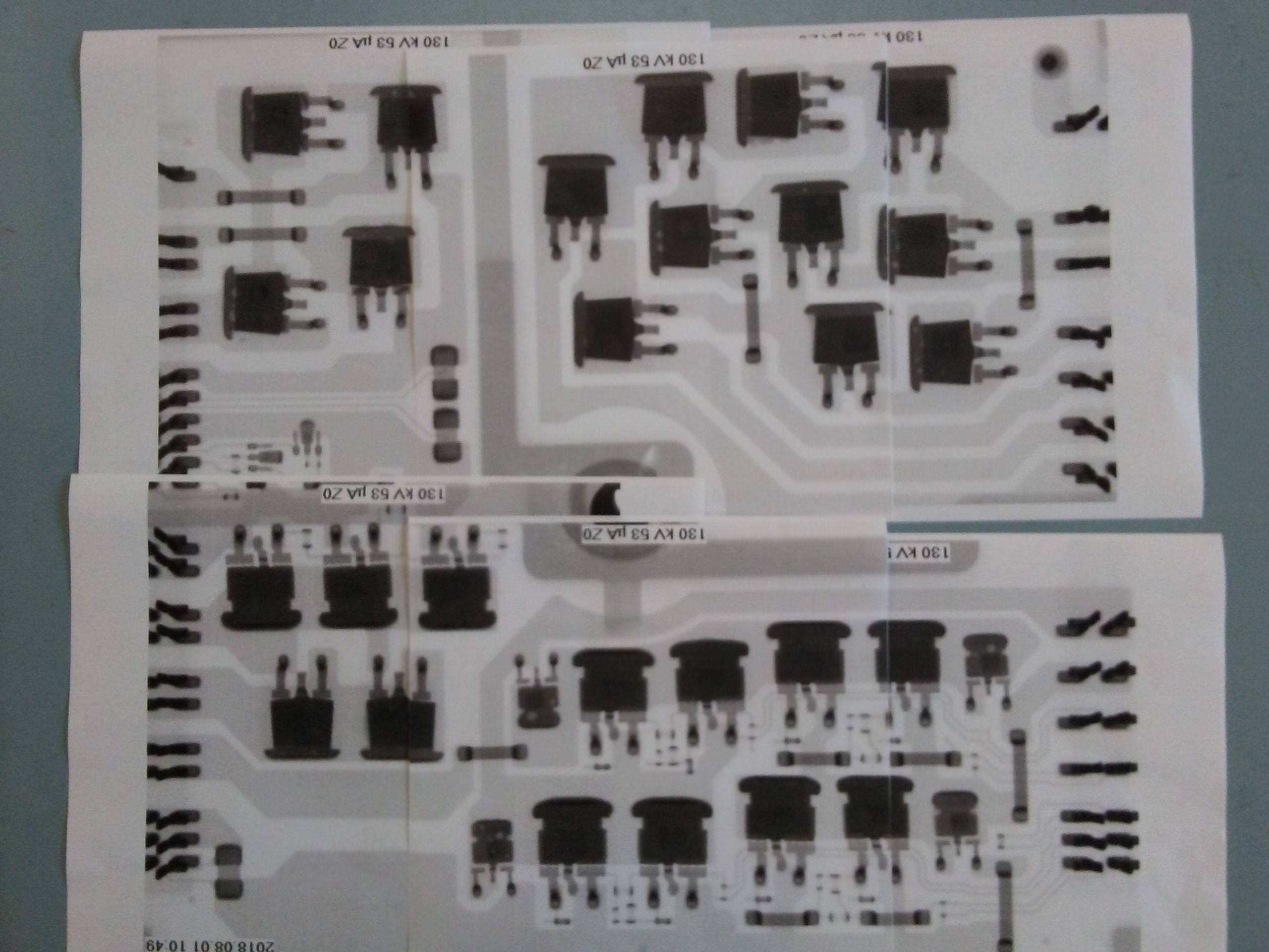
Edit: I'll go with IGBTs for the PFC stage; again one external back-diode per pair of IGBTs. Again, separate gate drive for the two PFC IGBTs.

The PFC diode is also two devices in parallel.
 
Hi Coulomb:
The DMM I'm using is a UNI-T CAT III I bought from Altronics rated to 1000V When I said cheap, that refers to price and accuracy of calibration, It's just not a Fluke if you know what I mean.

The 0.8 on the DIODE test that I am measuring is when the + of the meter is connected to the - if the Electrolytics, and the - of the meter is connected to the + of the BIG 3X Electrolytics. This would be showing the reverse of normal with a path going through both blocking diodes in series, and also these 2 are parallel to the 2 in the high side also. When I swap the meter leads to + to + of Electrolytic and - to - of Electrolytic, it says infenity.
In trying to check the 2 x 4.7 resistors in the doghouse, I can do a ohms check from the Neutral Input ring terminal and the other lead on pad 1 of the white strips, which would be measuring across just the 2x 4.7 resistors and the EMI Filter. I am getting a reading of 9.7R so the EMI Filter is probably adding the 0.3R If I apply MAINs AC Input, and check the voltage at these same points, I see a voltage drop of 1.57vac
At this same time, I have a clamp AMP meter on the LIVE AC line in, and it is only measuring 0.09amps Since it's not drawing much current,
This would make me think the 1.57vac is mainly being droped across the 2x 4.7R Resistors and the relay is still open?

The situation on the voltage across the 3x electrolytics being 348vdc and then gradually dropping, may be due to my MAINS source. My house is powered by Solar power only, so my Mains is actually from an inverter. This may result in some weird readings when there is a surge trying to charge the electrolytics, and they charge up to 348vdc but now that I've been brave enough to let it run a few minutes, it only drops to 345.5vdc and stays constantly there for the rest of the testing session. Depending on if its cloudy weather or batteries fully charged, I can see a few volts difference in output of the power inverter feeding my house, so that will vary results a bit. Some days I might see 239vac other days 241vac etc.

I like your idea of using the oscilloscope in dual trace diff mode. Saves me hastle of setting up the isolation transformer and less likely of getting BBQ'd. So if I'm probing around the 1K gate pull down resistors, what other point would I use as the reference point. would this be the + or - of the 3x electrolytics depending on if I was checking the high side or low side? These would connect to the emitter/drain of the power devices. Would the signals for the gate switching come in on pads 22 and pads 23?

Would it be worth unplugging the transformers, and in place of their primaries, temporarily put a 10w 10k dummy resistor.
This would give a 30mA current x 10k ohms = around 9 watts load, just to see if anything in the power devices work with a small load.

I might have to put the charger back in the car and connect the communications cable to it so that the controller PCB is happy before it will generate the gate drive signals. It might run for a few seconds before the error is detected and shuts down.
 
skylogger said:
The DMM I'm using is a UNI-T CAT III I bought from Altronics rated to 1000V
That's reassuring.

The 0.8 on the DIODE test that I am measuring is when the + of the meter is connected to the - if the Electrolytics, and the - of the meter is connected to the + of the BIG 3X Electrolytics.
Yes, that's what is expected. These are the two back diodes across the main IGBTs. I was still trying to work out why there was nothing on the 3 large electros. But you say there is 345-348 V there now, so that's fine.

I'd still like to see the 0.4 V from the PFC IGBTs. You should see this on the other side of the PFC diode, e.g. J21 to J19.

In trying to check the 2 x 4.7 resistors in the doghouse, ... I am getting a reading of 9.7R so the EMI Filter is probably adding the 0.3R
More likely your multimeter leads add 0.3 Ω to the reading. At 14 ARMS, the I²R loss would be 59 W.

If I apply MAINs AC Input, and check the voltage at these same points, I see a voltage drop of 1.57vac
Interesting. I think it could be out-of-phase inductive drop, but it might indicate resistance. There would be a spike of current when the capacitors charge up near the peak of each mains half-cycle.

At this same time, I have a clamp AMP meter on the LIVE AC line in, and it is only measuring 0.09amps Since it's not drawing much current,
This would make me think the 1.57vac is mainly being droped across the 2x 4.7R Resistors and the relay is still open?
As above, I just don't know. It depends on the leakage inductance of the EMI filter inductors.

The situation on the voltage across the 3x electrolytics being 348vdc and then gradually dropping, may be due to my MAINS source. My house is powered by Solar power only, so my Mains is actually from an inverter. This may result in some weird readings when there is a surge trying to charge the electrolytics, and they charge up to 348vdc but now that I've been brave enough to let it run a few minutes, it only drops to 345.5vdc and stays constantly there for the rest of the testing session.
Well sleuthed. I think that explains it exactly. So the front end seems to be working as expected, except that there is no PFC boost.

So if I'm probing around the 1K gate pull down resistors, what other point would I use as the reference point. would this be the + or - of the 3x electrolytics depending on if I was checking the high side or low side?
Use the negative side of the big electros, and measure only the gates for what you think are the lower IGBTs. It won't hurt to measure the upper IGBT gates, but if they are switching, then they will have the ~340 VDC square wave superimposed on them. The reference for the upper IGBTs will be their outputs; the IGBTs act on the base to emitter voltage, and the upper IGBTs are emitter followers. It might make sense to measure the outputs with respect to big electro minus first, to see if there is any activity. As mentioned earlier, I don't expect to see switching pulses without a CAN message to start charging, and that likely requires either the charger in the car, or some service aid that we haven't discovered yet. In the Elcon/TC chargers, you could insert a jumper and get artificial switching pulses for testing. I think we need a fair bit of Kenny-work before we get to that stage :mrgreen:

In short, there probably isn't much more that you can do till then.

Would it be worth unplugging the transformers, and in place of their primaries, temporarily put a 10w 10k dummy resistor.
I don't think so. Also, 9 watts in a 10 W resistor with no heatsink will get extremely hot.

I might have to put the charger back in the car and connect the communications cable to it so that the controller PCB is happy before it will generate the gate drive signals. It might run for a few seconds before the error is detected and shuts down.
Yeah. A slow test cycle, to be sure. It will be great to figure out some bench testing techniques.
 
Hi Coulomb / KIEV:
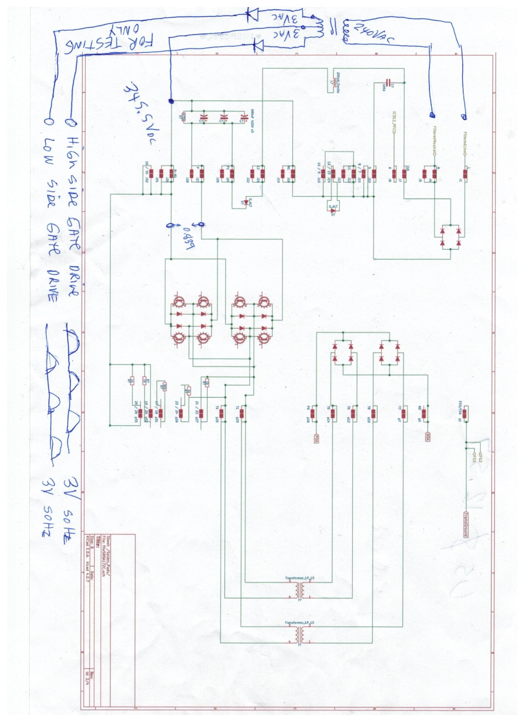
Would connecting a transformer with diodes as a test circuit like this drawing, allow to generate signals for the gates to allow testing of the IGBT's, or would this end up as a fireball of High side and Lows side switching on at same time? I figure connecting the test transformer primary to the active and neutral at the point it's already had EMI Filtering might work. I know centre tapped 3v +3v transformers are a bit hard to find. There are common audio transformers quoted as 1K PRI to 8R SEC ratio but they probably don't have the 350-400v rating. I'd also have to work out how to temporarily cut the true signals from the controller section so there is no chance of interference.
What do you think the original Gate signals look like? They probably would be around 3v but amplitude would vary according to charging current / voltage requirement. I've also heard that they normally use a higher frequency like 400hz or something to get more efficiency out of the smaller transformers. So just for testing, this should generate two 3v half wave 50hz signals 180 deg apart.

ju3WPlq.jpg
 
Back
Top