The Troubleshooting and Repair for On-board Charger (OBC) Thread

Mitsubishi i-MiEV Forum

Help Support Mitsubishi i-MiEV Forum:

This site may earn a commission from merchant affiliate links, including eBay, Amazon, and others.
AV7XQG9.jpg


Finally got the pictures to come up, Did not realize its literal text while editing the post, and picture does not appear until posted.
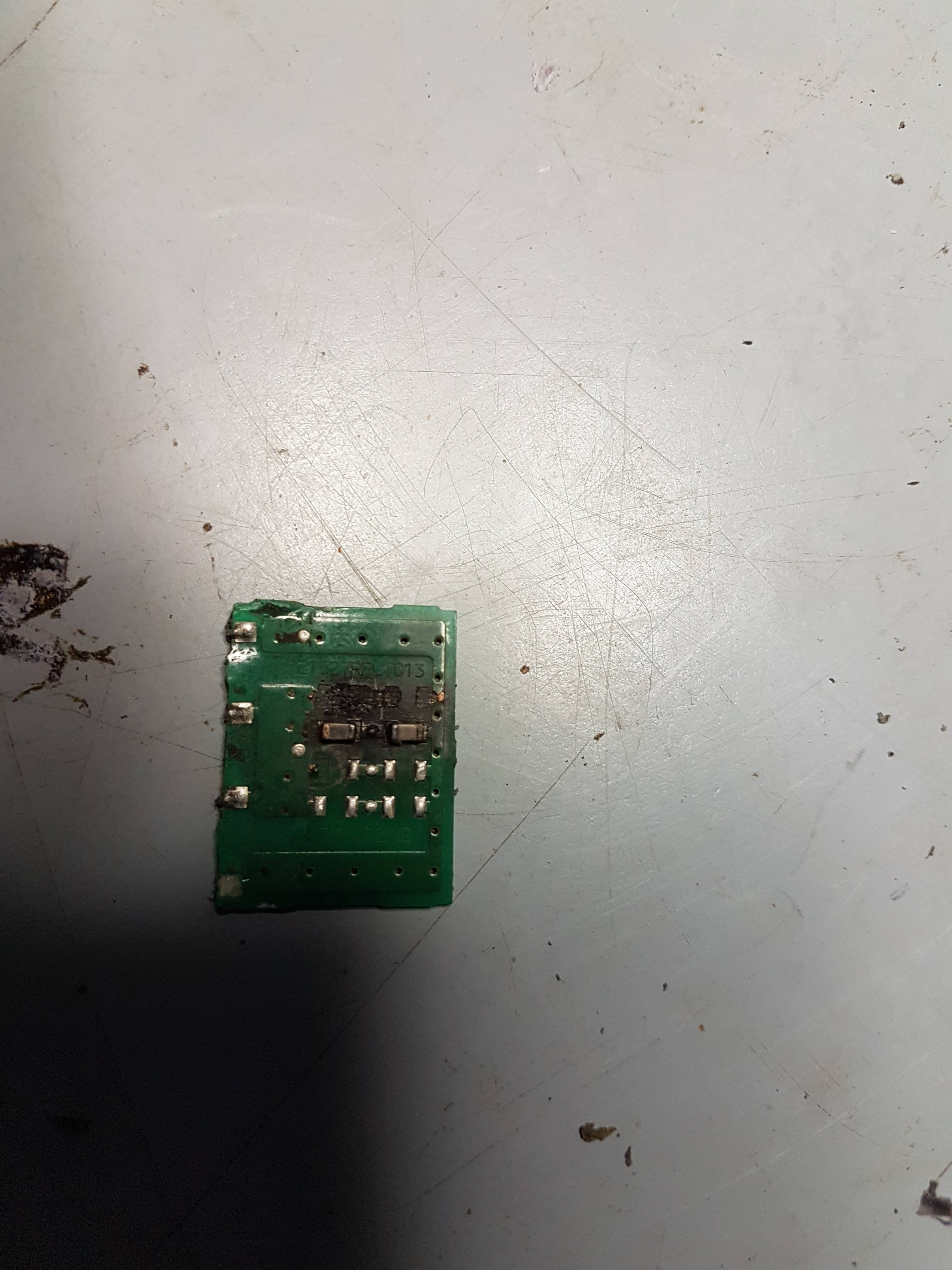
This is the daughter board that emulates the two blue thru hole caps. I think it originally had 4 caps on the board, with spare pads for other unpopulated caps. two of the four caps vaporized along with their tracks and pads. You can see the four square pads at the bottom that attach to pins that go into the Main PCB where C121 and C122 were originally. I left the pins in the main PCB, because so far I have been unable to completely desolder all the pins on the two white strips to be able to remove the power devices and heat sink.
A5OMcG3.jpg


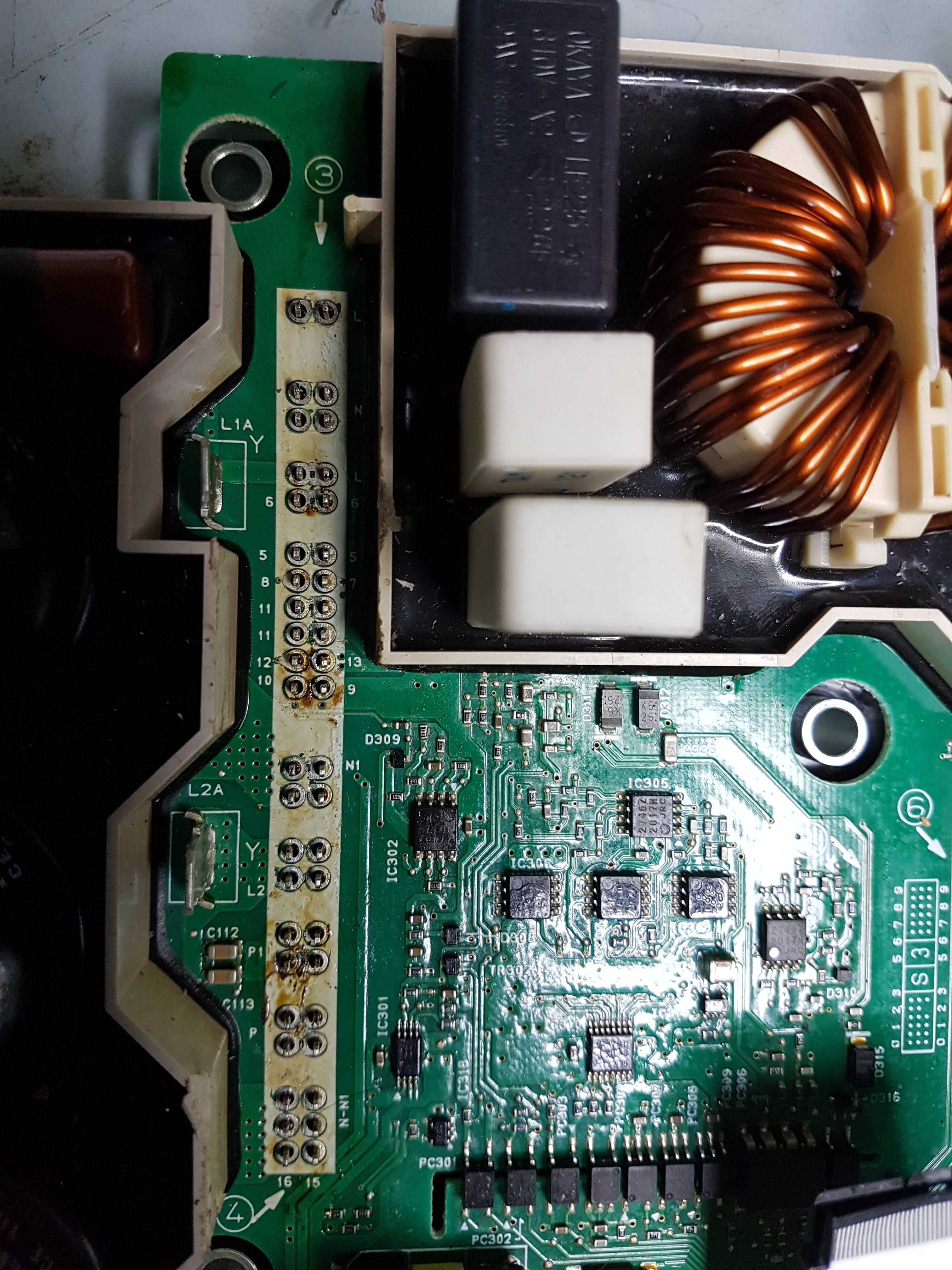
I having a really hard time getting all the solder removed from the holes along the white strips to be able to remove the power devices/heatsink. The solder sucker wasn't working, and I've done multiple sessions going over the pads with solder wick. There are still lots of pins still with small amount of solder, which means I can't leaver or pry without possibly damaging some tracks. I've used up a km of solder wick and will need to do some more shopping before I can do anymore work.

Originally I used an ohm meter across pairs of these pins and found quite a few with zero ohms so I thought I was seeing some shorted power devices. Upon closer look, There are quite a few of these pairs that have tracks between the pair of pads, so this was not a sign of a shorted component, I was just seeing the track between the pads.
jxX6wLU.jpg


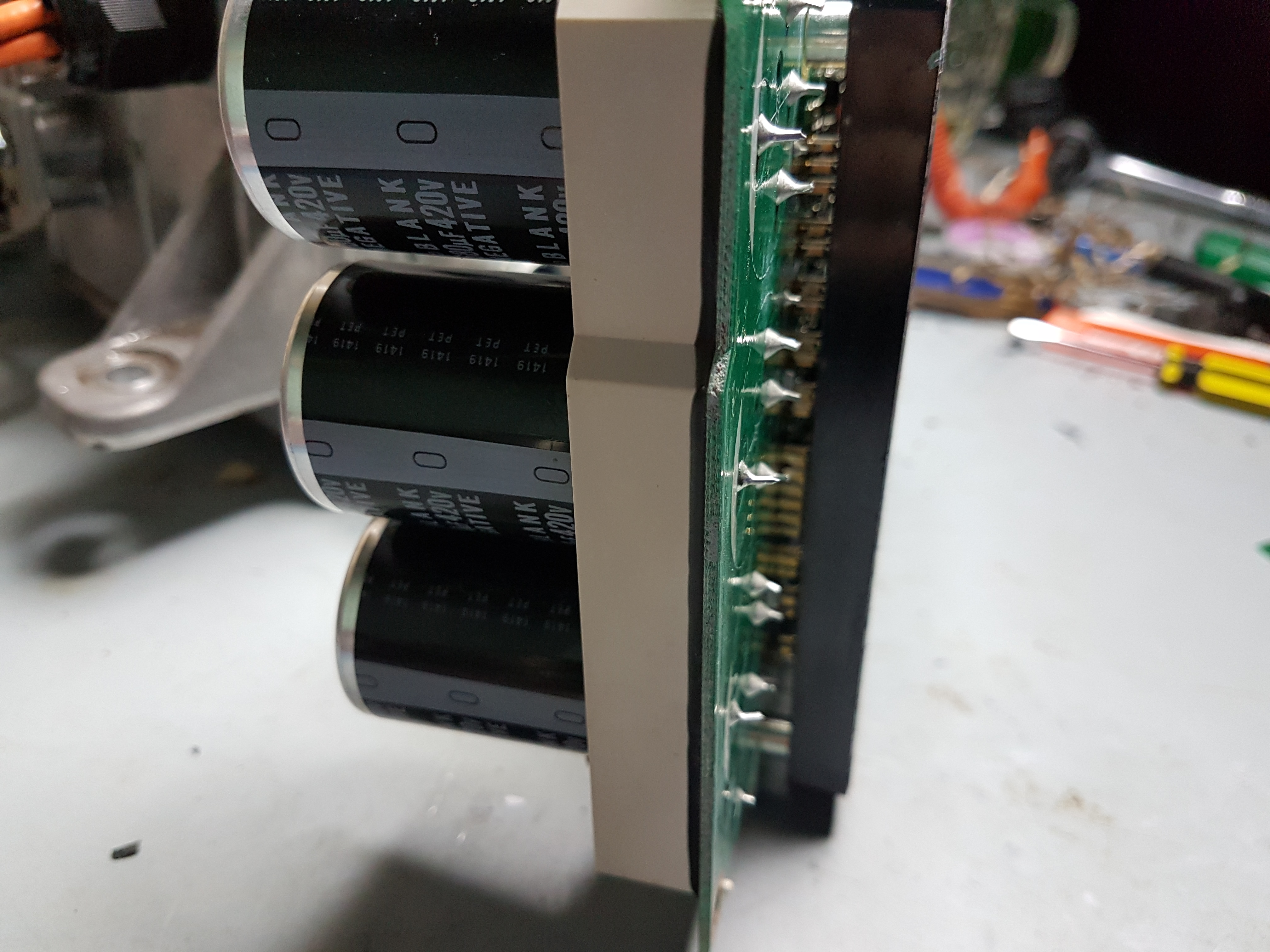
This is a side view of PCB and heatsink. To the left is electrolytic caps in doghouse, to the right, you can see some blurry gold pins/legs between the pcb and the heatsink. Those are the ones I am trying to remove solder from on the white strips on the PCB.
 
skylogger said:
You can see the four square pads at the bottom that attach to pins that go into the Main PCB where C121 and C122 were originally.
It looks to me that they are using 2S2P of surface mount capacitors to replace one through-hole capacitor.

Unless they had severe supply issues, I can only see this as temporary madness on the part of the manufacturer. The capacitors will have different leakages and capacities, so they won't share the voltage equally. Also, these SMD components won't be able to take any sort of overload gracefully, as we can see here.

What worries me is that we think that these capacitors are Y capacitors, i.e. one side is connected to chassis / mains ground. [ Edit: this was a guess which has proven false. The two capacitors, or two strings of 2S SMD capacitors, are across the charrger output.] So there must be some large transients on the mains that is over-voltaging them and burning them out. I would have hoped that other components would have protected these capacitors, for example the MOVs in the smaller mains conditioning box on top of the chargers.

But perhaps we're wrong about where these capacitors are connected, as there seems to be a correlation with the pre-charge resistor burning up. The chances of a mains transient in the second or so of pre-charge would be very small compared to the hours of charging, when the pre-charge resistors should be shorted by the mains relay. Hopefully, we'll find out soon.
 
bLNOfTC.jpg


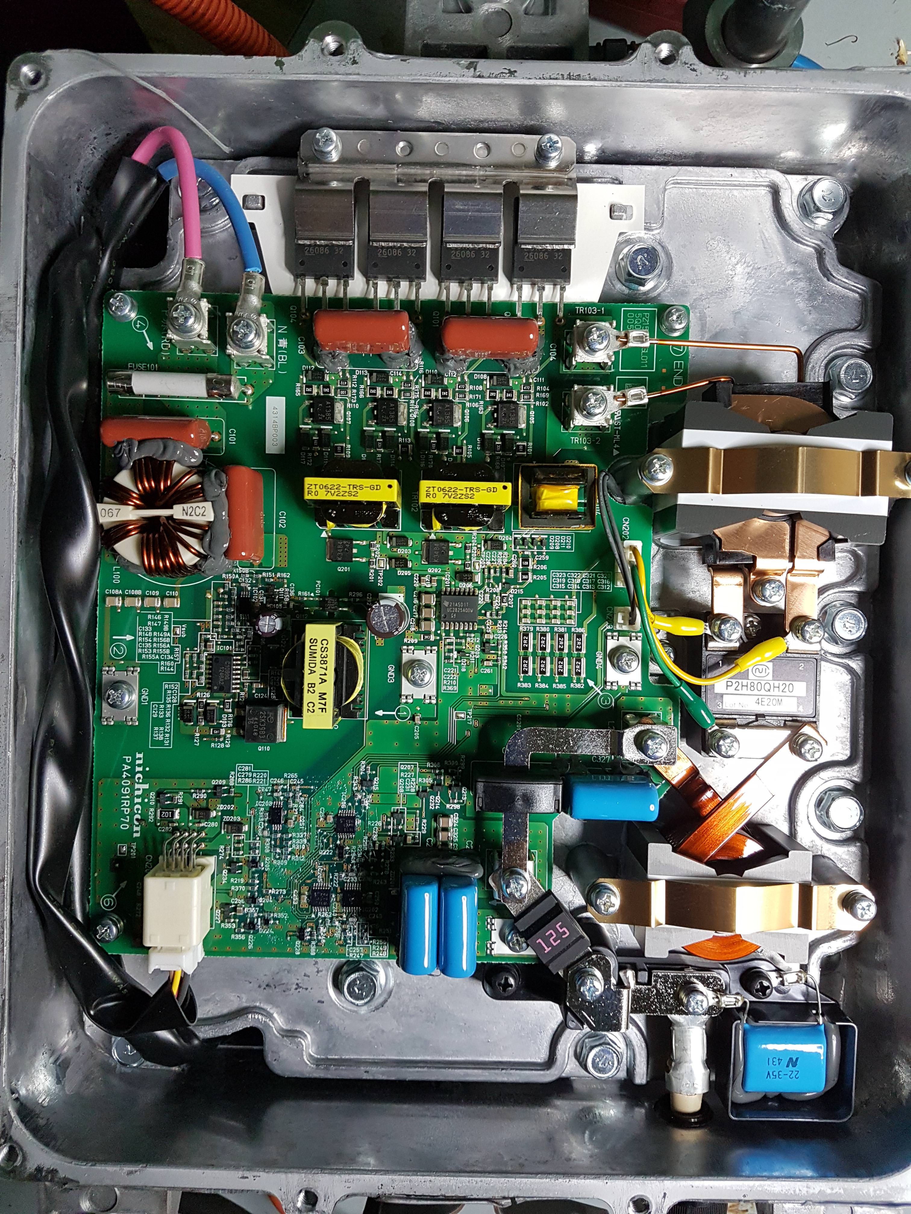
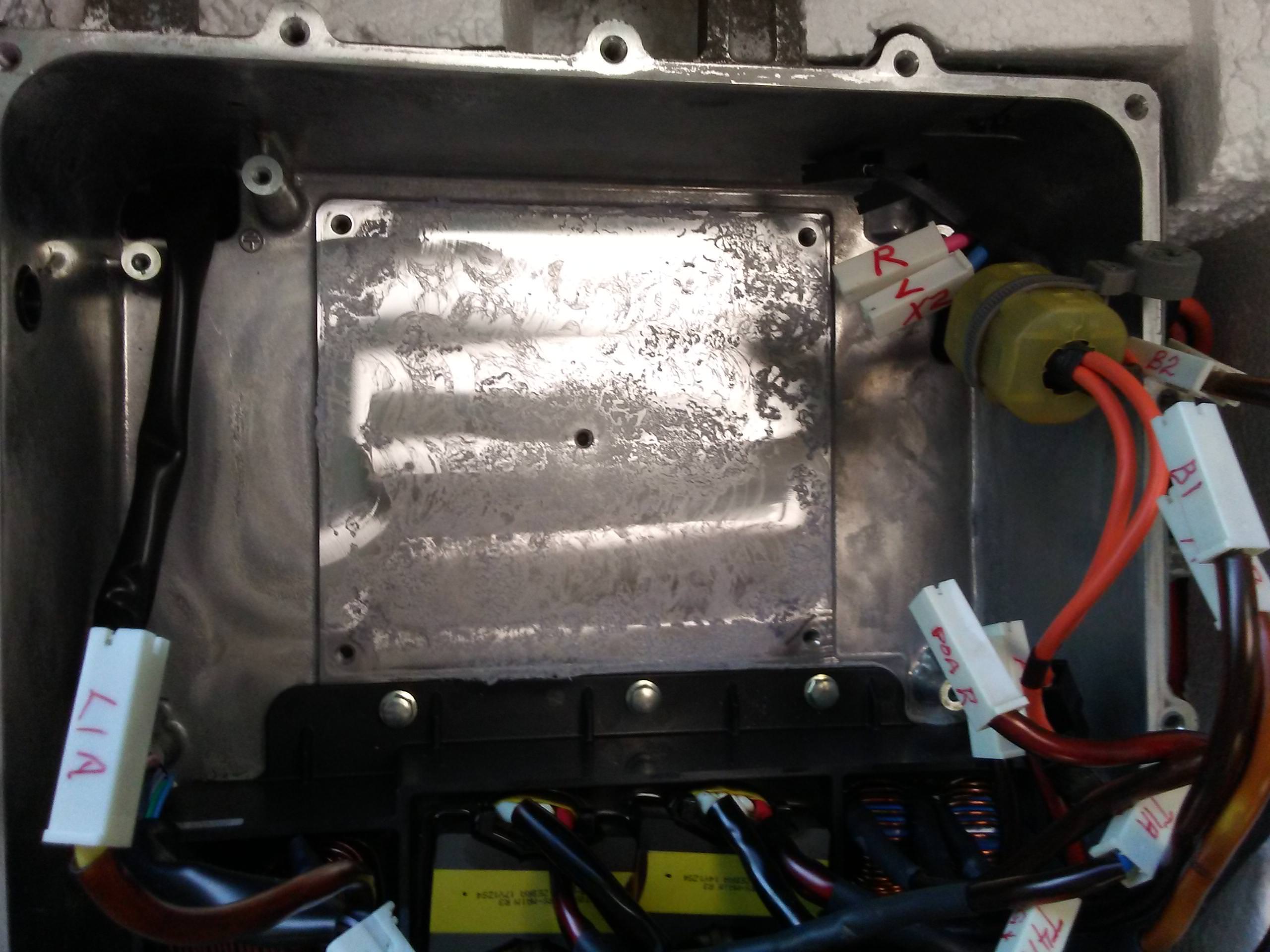
I've opened up the under side of the box where the DC-DC Converter is located. This picture is the result.
I've checked the Mosfets along the end of the PCB, and I've checked all the fuses onboard. visually there
are no places that look like smoke has been let out. I am thinking that any fault may be in the charger
section only, and because it blew the 20 amp fuse in the Inverter, that is why the DC-DC Converter is not
working at the moment. If the 20amp fuse is replaced and connecting the box (charger and dc-dc converter)
does not blow the fuse, then I may get 12v battery charging working again.
 
I tried desoldering the 100x leads from the main charger PCB to the heatsink, but could not get all the solder out of the vias.
I tried multiple sessions, but could not get every lead to wiggle as free, so didn't want to try prying and risk damaging any tracks.
Without seperating the heatsink from the PCB, I could not go any further with identifying pins since everthing within the heatsink
was potted. I ended up re-solder all these connections, and replacing the two caps in the doghouse filter section, re-assemblied
the whole thing and put back in the car. We replaced the 20amp fuse, filled up the coolant tank, and plugged back in the safety
plug and connected up the 12v battery. Connected up the MUT III Analyser, and had two errors being reported concerning OBC and DC-DC.
Ran the option to clear errors and re-test, and all errors were cleared. Checked the 12v battery before turning car on and voltage was about 12.3v. After turning the key and getting "READY" The Battery ICON and the HV fault Icons were no longer showing on the dash, and the 12v battery was now reading 14.4V so it appears to be charging. Connected the charging cord to the car and attempted to charge, but
could see the charge light on dash blink, then the HV Fault came on the dash, then both went out. It appears that even though the AC Charger still is not working, The MUT III Analyser was not reporting any errors. Just as a test, I tried to use the MUT III to ceck the hardware and software revision levels on the charger, and received a communications error. This leads me to believe that the PCB with the processor witin the charger is not working well enough to establish communications with other devices on the canbus. checked the canbus connectors but was still unable to resolve. As a test, we drove the car to a location that had a Chademo quick charger, and we are able to use the Chademo port to charge the car. So this now leaves options to try and repair the controller PCB in the charger, get a replacement charger PCB, Get a replacement whole charger/dc-dc, or buy a portable chademo external charger. Hopefully KIEV is sucessfull in doing something with the charger he is soon to receive, and this may give me a clue on how to proceed.
 
i haven't traced the circuits yet, just opened the top of jray's box to remove the boards.

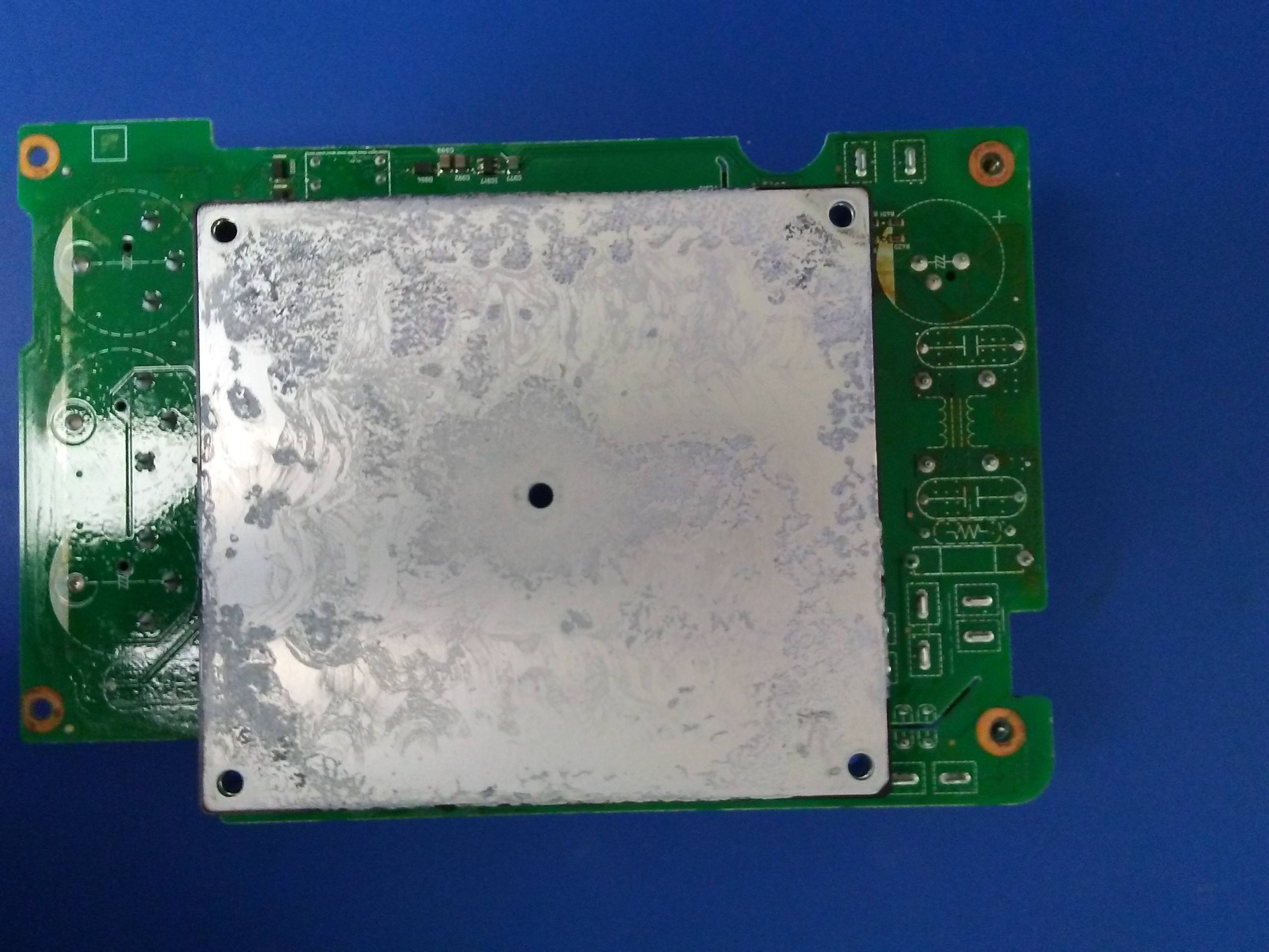
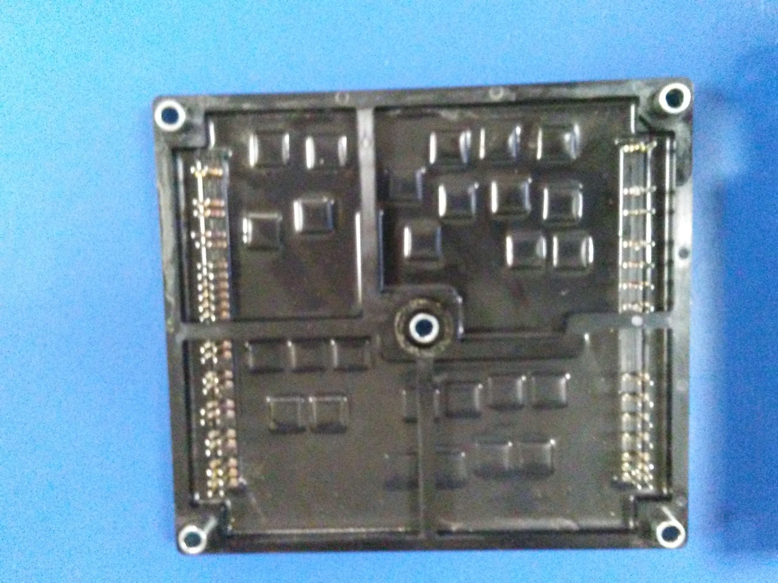
This is a view of the plate that attaches to the heat sink. It is covered with a thermal paste that is non-conductive electrically and is really too thickly battered in places--excess compound defeats the purpose.

65CYrdE.jpg


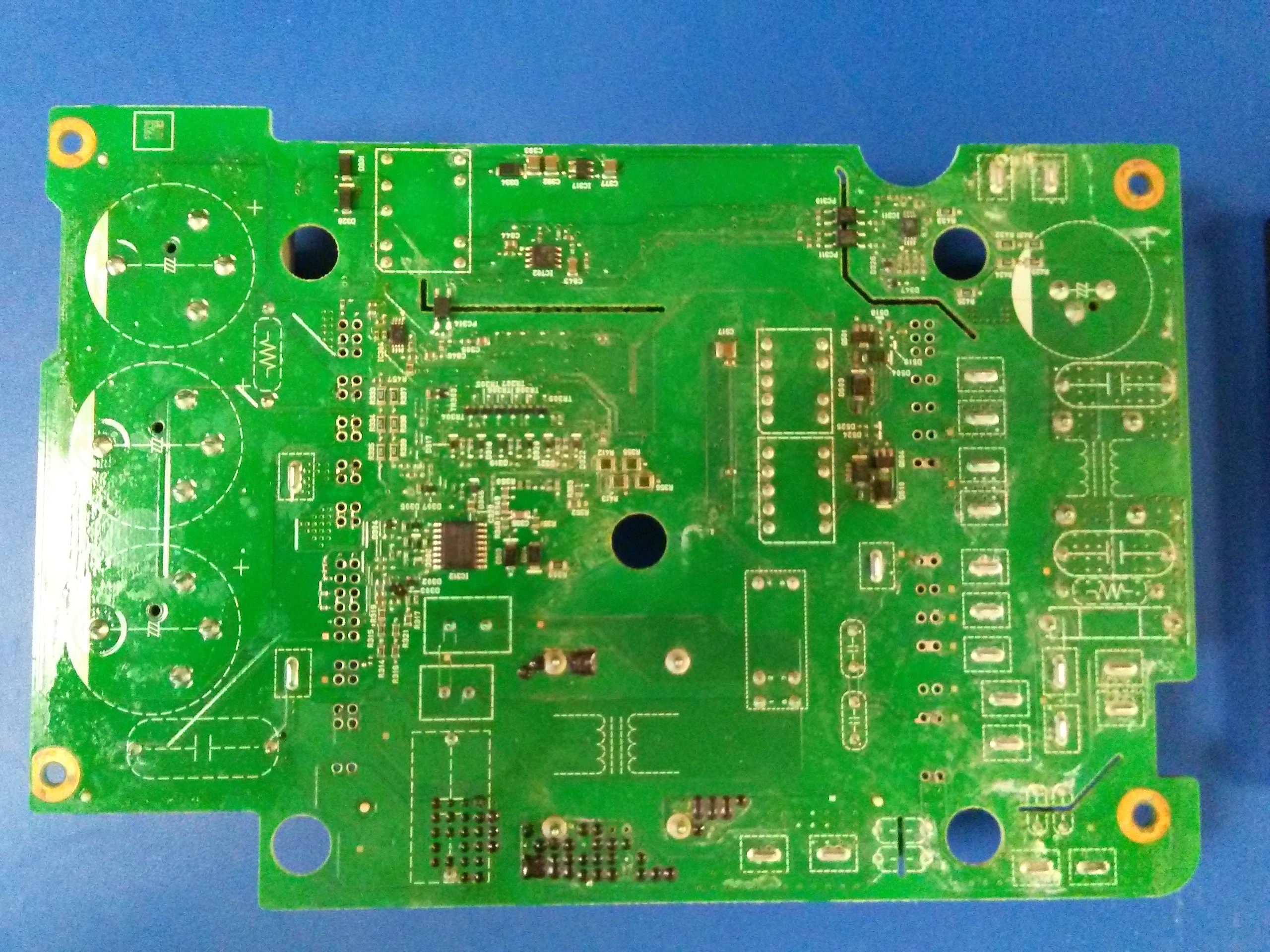
And here is the subject view without the plate after de-soldering 72 joints.

z9NcVgc.jpg


This shows what was hidden above the plate--and it's still hidden, buried under hard epoxy-type potting compound. Not easy to remove.

CXEyQ5t.jpg
 
Seems to be quite small and limited for such a big and heavy box with liquid cooling. Here is the heatsink area in the top plenum covered in thermal paste. i'm going to clean and check the flatness.

TnSb6NV.jpg
 
Jay's charger box has this nichicon part number on the bottom board, so we can use this as a reference designation as needed.

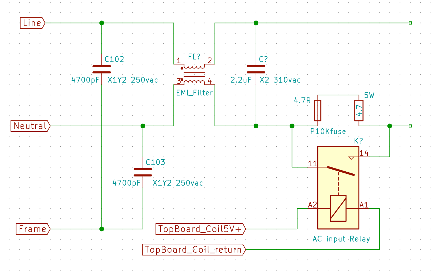
Here is the trace for most of the stuff in the bottom board potted region, aka the AC Input doghouse. The two big 4.7R ceramic resistors are connected in series and provide a bypass path across the relay contacts. These are made by Tamura, the larger one with green ink (TAM P10K series) is a thin-film current-limiting 10W fuse, and the smaller one with blue ink (TAM 7K series) is a wire-wound cement-filled ceramic housed 5W resistor. [Both were found cracked open on 1pk's board]. [edit to change 5K to 7K]

bJUQDQi.png


The only doghouse items not shown are the two high voltage (2kV, 1000pF) capacitors (C121 and C122, the blue M&Ms in jay's box and the SMD caps on a vertical board in skylogger's box), which are not part of the AC input at all. They are connected in parallel and appear to be snubbers on an inductor connected to a DC power buss, P0A.

[edit]
Using the daughter board with SMD caps is actually a smarter move than the thru-hole blue caps--it allows repairs without removing the big bottom board and de-soldering all the joints to get to the bottom side. And they even left a spare set of contact pads that can be used for the repair.


There seems to be 4 DC power busses on this board designated as: P, P0A, P1, P2.
 
Hi Kiev:
On your schematic of the Doghouse, you show the output of the drawing which will either be from the closed relay, or from the bypass resistors. If the pcb is still fitted in the box and heatsink still intact, so you cannot probe the bottom of the board, is there any points on top of the board where you can probe these output points while power is on, so it can be determined if resistors are ok, or relay contacts are ok?

There are two wires (a white and black) with quick connects that run from the top board down to the bottom board next to the dog house. Are these related to this part of the circuit?
 
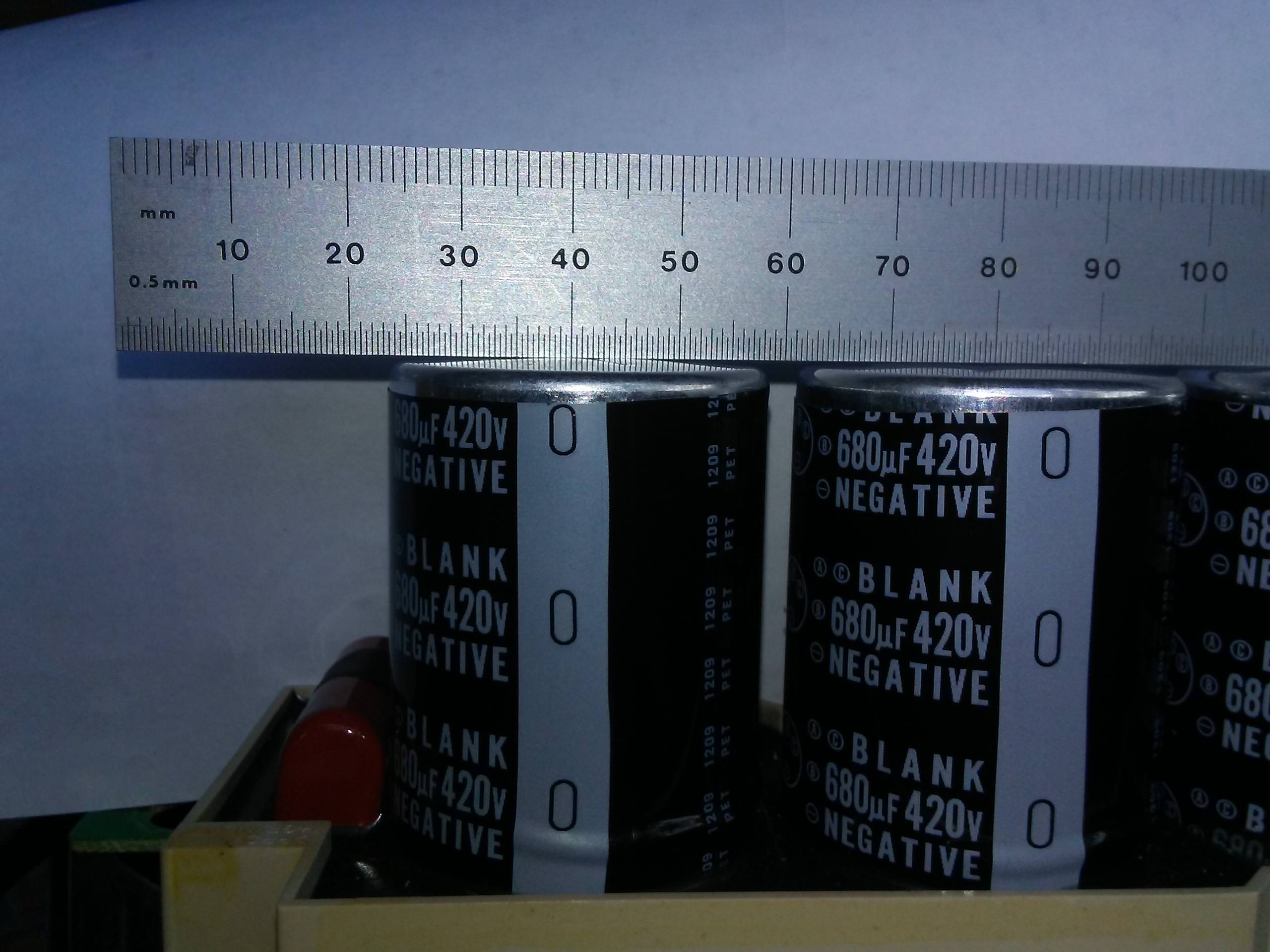
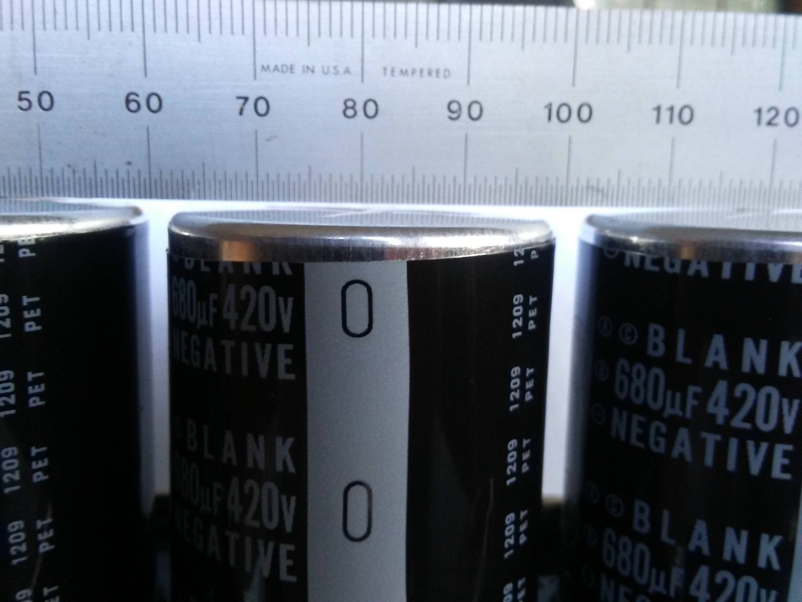
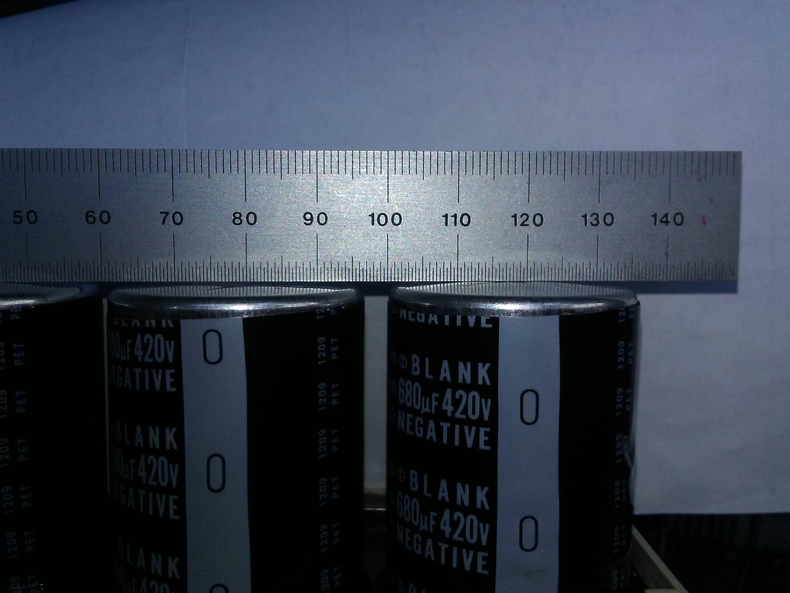
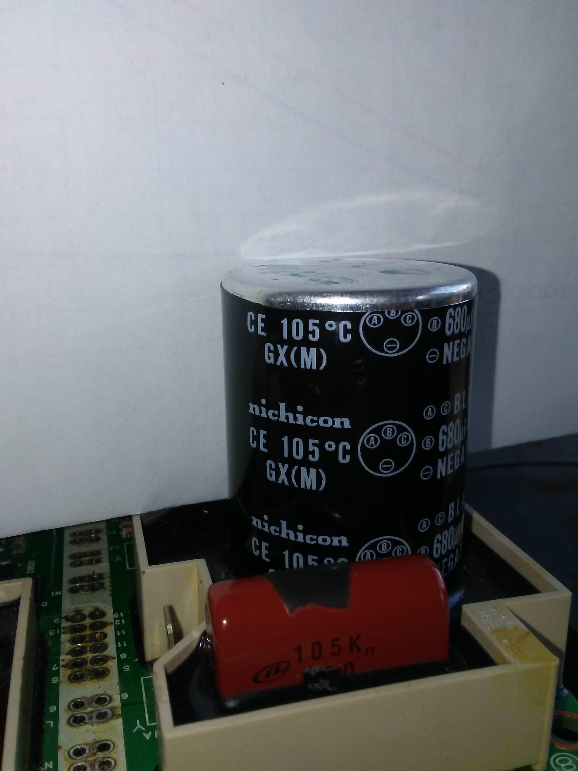
2 of the 3 big nichicon 420V 680uF capacitors in jay's box have bowed up the top dome of the relief valve/notch. i don't have a reference designator for them, so for now they are 1,2,3 from left to right, where number 3 is closest to the big hot inductor during charging.

kPrnDma.jpg


CWgHUYr.jpg


EVNVzhR.jpg


Gonna need some help finding these GX(M) with 4 solder terminals--i'm not having any luck so far.

X2eEGiQ.jpg


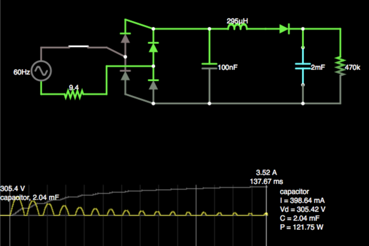
EDIT: Ran a simulation to see how long it might take to charge these caps using 340 pk AC voltage at 60 Hz.

pApI1Qq.png
 
Kenny, good work! Thanks for posting that related information on the other thread. You're right - these devices don't show up. Still looking...

Not much derating going on here... and if they're really only rated for 5000 hours at full voltage and high temp, some of us are there already. :roll:

A few questions:

1. What are the length and diameter in mm of these caps? From your photo I make it to be about 35mm dia.
2. I take it these are part of the output LC filtering and experience full pack voltage?
3. I don't understand their four-terminal configuration. Schematic?
 
JoeS said:
...

A few questions:

1. What are the length and diameter in mm of these caps? From your photo I make it to be about 35mm dia.
2. I take it these are part of the output LC filtering and experience full pack voltage?
3. I don't understand their four-terminal configuration. Schematic?


Howdy Joe,

1. Looks like 35 D x 55 H, for the body of the cap. It is using regular solder pins, not the Snap-in type.

2. i still have to figure out how to trace the waffle plate with the diodes and fets, but it appears that these caps hold up the first DC buss created by a diode bridge across the AC input and before the PFC circuits.

3. if you look at some of the pictures of the bottom of the bottom board you can see the 4 cap solder terminals. A and C are Blank (probably just for structural support, while B is (+), and the last pin is (-). This is likely related to the '(M)' option of the GX electrolytic caps, but is not shown on any datasheets so far.
 
kiev said:
1. Looks like 35 D x 55 H, for the body of the cap. It is using regular solder pins, not the Snap-in type.

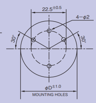
What's the lead spacing for the active leads? It should be 10, 22.5, or 25 mm.
Edit: It looks like 22.5 mm from the photos, but it might be 25 mm. I calculate 23-23.5, assuming that the dotted circle underneath the PCB is 35 mm. Oh! Some Nichicons come with 22.0 mm spacing. So it could well be 22 mm.

2. i still have to figure out how to trace the waffle plate with the diodes and fets,
Yeah. That might not be easy to replace. If a couple of devices shorts out, it might be necessary to replace them with discrete components on longer leads, bolted separately to the heatsink. Ick.

Then again, the hard epoxy might be the type that melts at a specific temperature, and you might find that those are standard components under there. But I suspect that they might be bare semiconductor dies.

but it appears that these caps hold up the first DC buss created by a diode bridge across the AC input and before the PFC circuits.
Right. So like the 2-3 capacitors in the PFC stage of the Elcon chargers, not like the one near the MOSFETs. Hopefully, they have proper snubber capacitors, perhaps on the Waffle Plate™. (I love that name :D )
 
JoeS said:
You're right - these devices don't show up. Still looking...
I think that this Rubycon capacitor is a pretty good fit. Better ripple ratings, same voltage, capacitance, diameter, and life, and Rubycon is also a good Japanese manufacturer. But it's 65 mm tall; will the extra 10 mm be a problem?

https://www.digikey.com/product-detail/en/rubycon/420HFG680MBN35X65/1189-3277-ND/6050306

tL9birk.png
 
skylogger said:
Hi Kiev:
On your schematic of the Doghouse, you show the output of the drawing which will either be from the closed relay, or from the bypass resistors. If the pcb is still fitted in the box and heatsink still intact, so you cannot probe the bottom of the board, is there any points on top of the board where you can probe these output points while power is on, so it can be determined if resistors are ok, or relay contacts are ok?

There are two wires (a white and black) with quick connects that run from the top board down to the bottom board next to the dog house. Are these related to this part of the circuit?

Howdy skylogger,

Here is a picture showing the solder pads to which the closed AC relay output gets transferred to the diode bridge down on the waffle plate--it should be mains voltage if the relay and resistors are intact. i would solder some small wires to the pins sticking up and run them toward the left wall and up above the top board where you could easily access them with a voltmeter. i don't think it would be safe to attempt a measurement directly on the pads with voltmeter probes.

Lx8sIFn.png


The AC gets filtered in the small box screwed to the charger cover, then goes into the charger to the top board and thru a surge supressor and filter, then thru the white and black jumper wires down to the bottom board to the relay doghouse, then thru the relay to the solder pads in the picture above.

In the upper left quadrant of the waffle board are 4 diodes that rectify the AC to create the first DC buss.

CXEyQ5t.jpg


The diodes are DF25V60, 600V 25A SMD rectifier diodes made by Shindengen.
 
kiev said:
The diodes are DF25V60, 600V 25A SMD rectifier diodes made by Shindengen.
Ok, I'll bite :)

How the hell do you know that?

Is there a PCB under the potting on the waffle plate™ ? How does the heat get from the components to the plate?
 
Hi Kiev:
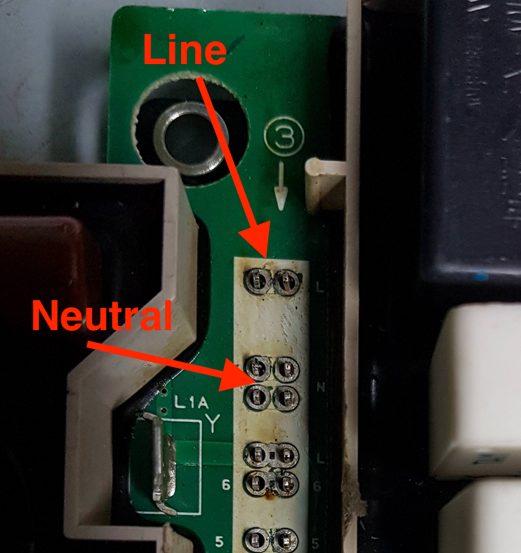
The charger that I am working on is back in the car, at a friends house, so on my next visit there, I can do like you say and solder a "LINE" and "NEUTRAL" wires out to a point I can connect a volt meter to and fire it up. Just to be clear, Your Arrow pointing to "LINE" is sorta pointing between the two pins, so I guess this means these two pins/pads are connected together? I know once I get there I could scrape the solder mask off, but I figured you already knew and it would save me scratching around inside the box. Also the "Neutral" arrow you drew, is pointing in the middle of a group of 4 pins/pads. Are all 4 of these joined together, or should there be one out of the 4 that is the Neutral point.
I guess if I had a storage oscilloscope, I could see the soft start, with a voltage a bit lower than 240vac (I'm in Australia) and then when the relay closes a second or 2 later, I should see the full 240vac at the test points you pointed out to me if the relay is working?
 
@coulomb,
i used an xacto knife to scrape the epoxy off the diode. It is a very brittle material, and in a thin layer it can be levered off with a blade. Also i use a hot solder iron on thicker sections--the heat pulverizes the surface to a gray powdery dust. So heat and scrape, rinse and repeat until down to the chip.

The upper right quadrant has 10 chips, 3 of them are DF20L60U fast recovery diodes. i haven't drilled down to a board yet, but surmise there is some sort of pc board under the epoxy to which the parts are soldered. The aluminum bottom plate is 2mm (0.08") thick and measures 5-3/8 x 6".

[edit] uh oh, it appears that the FETs or diodes in the lower half are different size devices, and the tops have been etched to remove the part numbers. Why such security measures deep in the bowels of a charger...?


@skylogger,
yes you are right on all questions--almost all of the pads are connected in pairs with a fat trace below the solder mask. The "neutral" (usa 120vac) cluster of four are all connected together also. It could be labelled "line2" for 240vac such as we use for Level 2 charging. [edit for usa mains power]
 
kiev said:
It could be labelled "line2" for 240vac such as you use there.
Actually, we (and nearly every country outside the USA and Canada) have one line and one neutral; the neutral is earthed at the main switchboard by a neutral to earth link. We just don't have center-taps on our 240 V transformers. All our general purpose outlets are 240 V (occasionally 415 V), none are 120 V.

We're supposed to be converted to the international standard of 230 V, but we comply by saying our tolerance is -5% to +10%, or some such. In practice, I've never seen it below 240 V here. I see that the USA has no interest in following the international standard, i.e. 230 V and 115 V.

@kiev, Thanks for the info on the waffle board™. A photo would be great; perhaps when you have more gunk scraped off. Did you consider an oven? A few minutes at around 100-120°C would not hurt the semiconductors, and might save a lot of time crumbling off the coating. I've heard that some of the thicker and/or harder potting has to be melted off; perhaps Kelly controllers are like this?

Any thoughts on what to replace the coating with when it's ready to be fired up (so to speak)?
 
Back
Top