The Troubleshooting and Repair for On-board Charger (OBC) Thread

Mitsubishi i-MiEV Forum

Help Support Mitsubishi i-MiEV Forum:

This site may earn a commission from merchant affiliate links, including eBay, Amazon, and others.
The connection between R720 and R721 is ok. There was a connection remaining from R720 to Ground, but after removing the resistor the Ground solder pad of R720 is now gone. I'll have to bridge it with solder or a wire when replacing the resistor (see 3rd picture below).
Besides of the R720 I also removed the Ground layer in the area that was marked in red in my last post to be sure that there wasn't a short in this area. Now I can say: there wasn't a short in this area. The VIAs in this area still have a Ground signal that must come from the top side of the board.

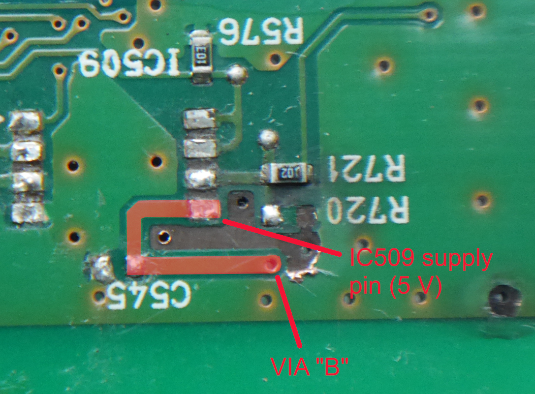
I traced the way of the 5V-signal from the TR710 to the VCC of the IC509 based on what you have told me. The following pictures are showing it:
Starting on bottom side...
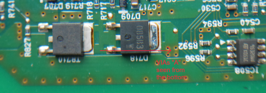
4osKaib.jpg


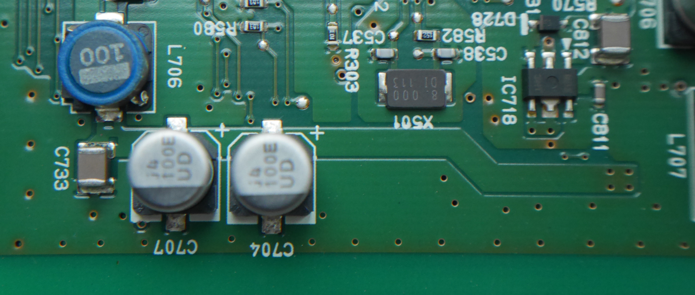
... continuing on the top side... [edit: VIA "C" isn't a VIA, kiev corrected this wrong assumption in the next post]
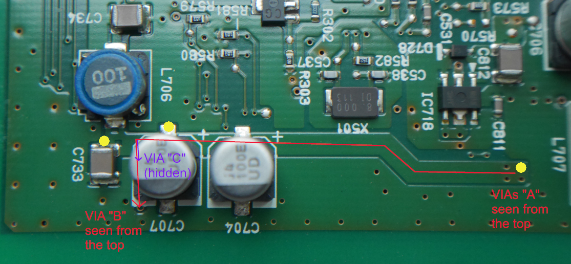
7tjFPeX.jpg


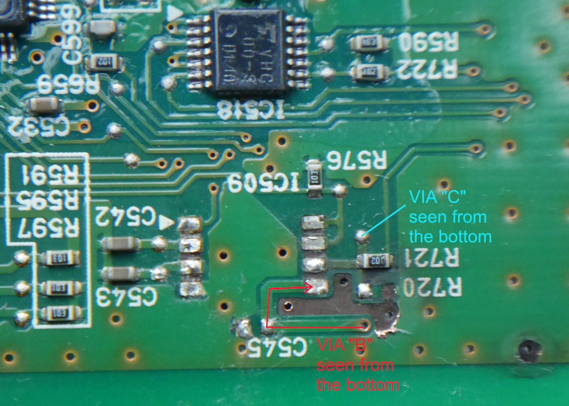
... ending on the bottom side again. [edit: VIA "C" isn't a VIA, kiev corrected this wrong assumption in the next post]
eisX4Rs.jpg


Taking some measures on this circuit, I noticed a high resistance (1.125 kΩ measuring in current flow direction or 8.96 kΩ measuring in opposite direction of current flow) measuring between VIA B and the places marked by a yellow circle in the second picture (top side). The resistance between VIA B and VIA C (measure taken on the bottom side of the board) is 1.185 kΩ. The resistance between VIA C and VIA A (measure taken on the bottom side of the board) is 2.7 kΩ when measured in opposite direction of current flow, or 10 kΩ when measured in current flow direction. I don't see a good reason why there would be high resistance in a supply line. The VIA C and the trace going to the VIA B are both under the C707. [edit: VIA C isn't a VIA, kiev corrected this wrong assumption in the next post] So either the traces don't run as I believe they are running, or there is some sort of resistance there that had been designed to be there (under C707! - seems unlikely...), or there has been some damage, what doesn't seem unlikely as two of the 3 impacts are directly on the other side of the board.

I also took some resistance measures on the TR710 but it doesn't seem suspect (yet). I measured 220 Ω between both legs, 530 Ω between the metal tab and the ground leg and 780 Ω between the metal tab and the other leg. IC509's VCC to the metal tab of TR710 measures 533 Ω, what is consistent with the 530 Ω between the metal tab and the ground leg of TR710 + 3 or 4 Ω between IC509's VCC and Ground.

Thanks for the soldering trick. I struggled less today when I've removed the R720, but it might have been luck or because one side wasn't really holding it any more. I have some solder braid around but it isn't absorbing the solder. Maybe it misses some flux or my soldering iron isn't powerful enough to heat up enough braid and solder. I'm a bit more successful with the (manual) solder sucker, but it's not the tool to get the little rest of solder away or to be used in very narrow spaces. The other difficulty with narrow spaces is that I'm always afraid to create solder joints where there shouldn't be one (neighbour parts and legs, ...).
 
Does your meter have a diode check function? That is what is needed to check transistors and diodes.

The pad you marked as "A" is the 16V supply that is created by a PWM Boost circuit from the 5V supply. Is the 5V supply still shorted to the Ground plane with the legs of the transistor lifted?

The point marked as via C, is just a test point trace used to measure the voltage into the IC--it is not a via and doesn't pass thru the board.

Flux is your friend for soldering and rework, wicking, etc. The boards are made with lead-free solder and it doesn't seem to flow as easily as the old leaded stuff. Small gage wire can be stripped back and used as wick also--heat the wire and hold it to the excess solder to be removed, the solder will flow (wick) toward the hottest region.

The input to IC509 thru R721 comes from a NAND gate IC504 that is monitoring for the presence of the 5V HATT. If that supply doesn't exist then IC509 will not allow the microcontroller to operate.
 
I haven’t been able to check the transistor accordingly, as I didn’t make it to get a leg desoldered. It was as if an invisible layer was avoiding that the solder in place and the solder I added were mixed up. The solder in place didn’t want to melt... So, I was pushing around my liquid solder ball again and again against and around the solder pad and the lead, but all I achieved was to create several solder “nuggets” without having any impact on the existing solder connection. I’ll try it again in a couple of days after having cleaned the leg with some alcohol and having got a more powerful soldering iron. I had this same issue when I tried to desolder C707, that is still in place too. But enough words lost on inglorious solder work stories: this is not the topic of the thread...

I got a bit confused about the 16 V supply you were talking about. I thought the IC509 is powered by the switched 5 V source. And I thought the signal coming from TR710 and through D718 was this 5V signal. How else would a 5V signal come to the VIA that I marked “B” and that runs to the VCC of IC509? I added a picture with markings again to make my question clearer:
Tracing the 5V from the consumption to the supply we start at the VCC pin of IC509, where we have 5V. We go further to VIA “B”, where we also must have 5V.
qdSgVPK.jpg

We flip the board and go over to the other side where we find our VIA “B” again, at 5V.
CPiU5dT.jpg


K08Who5.jpg

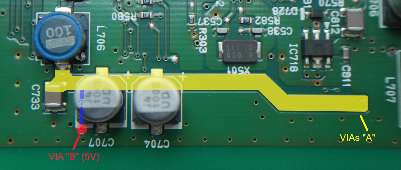
There the guessing starts. There is no trace visible that runs to the VIA “B”, so it must come from under the C707. I don’t think that there is a complicate circuit hidden under the C707, I doubt that there could be hidden anything more than just the trace supplying the VIA “B” (running like the drawn blue line in the picture). But this would mean that the VIA “B” would be supplied out of the area marked in yellow, and that would mean that this area should be at 5V. But now you’re saying that the VIAs “A”, that are also in this area marked in yellow, are...
the 16V supply that is created by a PWM Boost circuit from the 5V supply.
And this would mean that the area marked in yellow would be at 16V. But how could the VIA “B” then be supplied with a 5V signal? Maybe you can bring some light into the darkness here...

But this place on the board is also interesting for another reason. Downwards the circuit, towards consumer, from VIA “B” to the VCC pin of IC509 I’m observing what is supposed to be a short with only 4 Ω resistance against Ground. On the circuit upwards, towards the supply, taking measures from different contacts in the area marked in yellow, I’m observing much higher resistance values against Ground, so I wouldn’t expect a short to be present there. What is surprising is that the measured resistance changes, depending on with which probe of the meter I’m contacting Ground and with which the conductor. In one case I’m measuring 1.25 kΩ and when I switch the probes and take a measure from the same measuring points, I get 8.96 kΩ. I’ve reproduced these measures many times, as I had difficulties to trust them, but the results were reliably the same. These values also correspond to the resistance measured between the different contacts in the area marked in yellow and the VIA “B”. At least that would be consistent as then at the VIA “B” there’s almost no resistance any more against Ground. I can’t explain it. But even with this limited understanding of what happens there, I guess that some deductions can be made. Now again I can’t be sure that VIA “B” is indeed connected to the yellow area, but if it is kind of a more or less direct connection, than it seems likely to me that the short could be in that area covered by the C707. So, I’m looking forward to what I’ll find when I’ll finally make it to desolder it!

Thanks for rectifying my wrong assumption that “C” was a VIA. I’ve added an edit to my earlier post concerning this to not mislead later readers of this thread.
 
iOnico said:
...
And this would mean that the area marked in yellow would be at 16V. But how could the VIA “B” then be supplied with a 5V signal? Maybe you can bring some light into the darkness here...

Great pictures, but you are getting off in the weeds. There is no need to remove C707, it is the 16V supply filter cap.

TR710 (2SC3518, NPN Silicon Bipolar Transistor) is part of the Boost circuit to create the 16V supply, which you have marked in Yellow.

Keep it simple: Did you have a short (very low resistance) between Via B and the Ground plane? And has it changed since you removed IC509?

The 5V supply is used all over the board on both sides; there is an internal plane layer that carries the 5V and it can be brought up to the surface layer with a via wherever it is needed.

My concern is that you may have a shorted 5V layer to the ground plane layer as they are only separated by a thin layer of fiberglass and glue; a high energy arc can punch thru the layers, melt metal and created short circuits. If your board is shorted then there is no need to continue with it, find a used board and swap it out.

Is there any metal splatter shorting pins 90 -100 of the microcontroller? Pin 99 has a via connection to the 5V. Might be good idea to carefully inspect all the ICs for small metal splatter ball shorting of pins.
DxJpCxE.jpg
 
That information about the 5V being carried in a sublayer of the board changes everything, indeed. You might have noticed it: I’m not used to work on PCBs and so I don’t know if this is common knowledge and if it’s usual that this kind of boards have such supply layers. So, to have got this information was like if a magician had betrayed its trick to me! :eek: Suddenly many things make a lot more sense...

I suppose that you already had more than just good basics about electronics when you started “studying” the iMieV. But how many cars and boards have you analysed to accumulate this knowledge? I’m still deeply impressed and very grateful for the help you offer by sharing this knowledge!

Unfortunately, your last diagnostic is bad news for the board, as this low resistance of 4 Ω (the short) is still there between VCC pin of IC509 and Ground, even after having removed IC509 from the board. I also haven't found any metal splatter neither on the pins of the ICs, nor somewhere else on the board. The major surface where the microcontroller and the ICs are situated, is also covered by a layer of varnish or transparent glue. Not sure it might have been enough to stop a hot metal ball arriving with high speed, but it might have given a bit of protection.
I’ll start posting in EV forums that I’m looking for a replacement control board and if someone has a wrecked iMiEV, C-Zero or iOn around, where this board is still intact. Do you know if I need to fear compatibility issues or some checks of serial numbers, part or car IDs or something? Do you have some hints where you would start searching for such a board?

Back to my damaged board. As there are only three impacts where the arcing occurred and as the board isn’t usable any more anyway in the state it is right now, I’m tempted to drill holes through the board at the places of the arc impacts (diameter a bit larger than the VIAs). If the cut would be clean on the edges, I could imagine (in theory) that I could drill away the place where the layers are melted together without creating another joint. Would be pretty experimental and, I admit, not really promising, but I guess that I don’t have a lot to lose any more on this board.
 
iOnico said:
I’m tempted to drill holes through the board at the places of the arc impacts (diameter a bit larger than the VIAs). If the cut would be clean on the edges, I could imagine (in theory) that I could drill away the place where the layers are melted together without creating another joint. Would be pretty experimental and, I admit, not really promising, but I guess that I don’t have a lot to lose any more on this board.
Interesting idea, and I think it should work. But I think it will turn out to be another chip drawing way too much power. I'd be tempted to power it up with 2-3 V on the 5 V supply, and find out what is warming up with a non-contact thermometer. Then you probably don't have to butcher the PCB.

Of course, if it really is a short between layers, that won't help. But it should not be too much trouble. If it turns out to be only one or two other chips or components, you might even be able to repair it still. The chances are low, so it might pay to put out feelers for replacement boards in parallel.
 
If your meter has a continuity beeper, then you could solder a small wire to the metal tab of TR710 and one to a good ground location, then connect the meter and it will begin beeping.

Using a pin vise or small hand-held drill chuck with a tiny drill bit (0.5 or 1 mm), you could twist the bit by hand and slowly work your way down the ground vias near the "B" via, possibly cutting thru any shorted layer such that the beeper will stop. Drill a little, then remove the bit to check the beeper, then repeat until the beeper stops or goes thru to the other side, then try the next one. The two vias closest to R720 are prime candidates.

There are numerous lands and vias with the 5V supply that you could then solder a wire and run it over to the trace at C545 to connect to Vcc. Replace the IC and you might be back to charging.

i don't know how much the shipping would be, but if you can't find a board over in Europe, then i could probably find one over here in USA. i bought a used OBC from Japan and the shipping far exceeded the cost, plus it was a hassle getting thru customs.

there is no issue with using another board from any of the triplets from the same year or OBC generation, no VIN or serial number. Is your board a Nichicon PZ1546R002?
 
Thanks to both of you for your helpful advice for the next steps. I’ll try to find a non-contact thermometer somewhere and then search for the place with significant heat dissipation with 2-3 V being supplied to the 5 V circuit. If it’s finally a short in layers at one of the VIAs having been impacted by an arc, I may still observe some heat dissipation there, what would allow me to refine the order of the VIAs for drilling. If I have to drill, I’ll definitively want to do the “direct feedback” method you have suggested by having the permanent continuity check in place. That’s a good idea to avoid drilling more in depth than needed.

If I get to the point to really find and remove the short, I’ll see if I’ll have damaged the 5V layer in a way that I’ll need to bridge the 5V supply from IC509. But what is sure, is that I’ll have to replace C545, that I’ve lost in the solder ball, I’ve put around it, when unsoldering it from the board. What kind of capacitor could I use for the replacement?

I’ve started looking around for a replacement board or a whole OBC-DCDC-box. Best would be indeed to find it in European Union to not have customs questions to deal with. Thank you, Kenny, for your offer to search one in the USA if I don’t succeed over here.

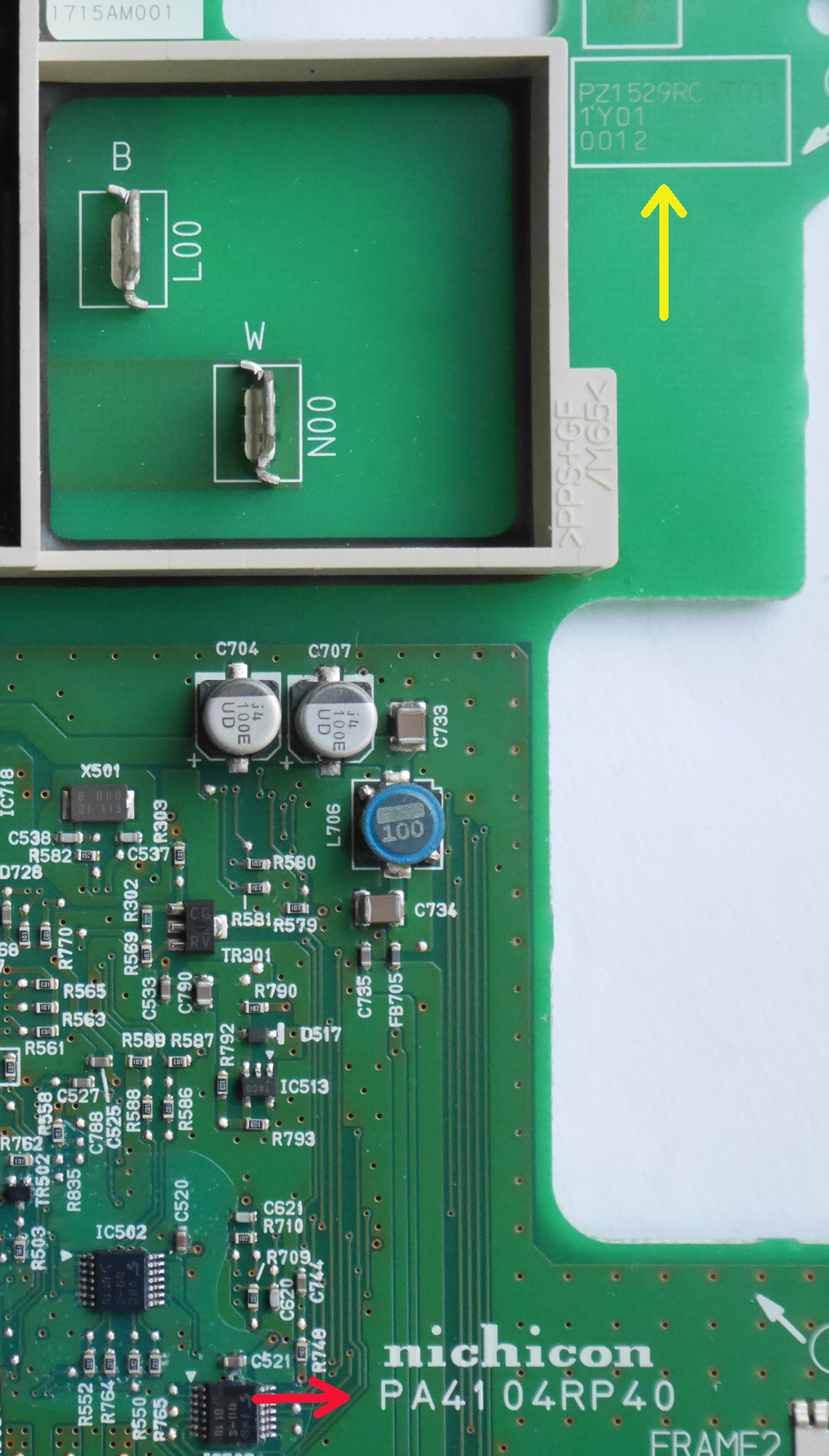
Concerning the identification of the board, there are two numbers on it, both having a format that is close to the number you gave in your question. I suppose that the relevant one is the one marked by the yellow arrow: PZ1529RC NT011.
laRspB8.jpg


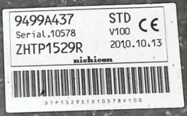
I found a used OBC-DCDC-box from a wrecked iOn in the Netherlands: a professional parts reseller offers it for 700 €. It’s less than 10% of what the Peugeot dealership wanted for the repair, but having in mind that I just need one board out of the three, it’s still some money. So for the time being, I only consider it as a fall back solution. This is the label of the OBC-DCDC-box that is offered by the parts reseller:
smyWxhW.jpg


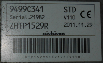
And this is the label of the OBC-DCDC-box in our car:
57gnycW.jpg


Obviously the OBC in our car is one year younger and it’s V110 against V100. I have no idea what changed from one version to the other and if this allows or not to transplant the control board. Can you say something about that?
 
Those appear to be the same OBC based upon the Nichicon part number, ZHTP1529R.

The Japanese version boards that i bought have an extra fuse on the AC inlet and a EMI filter inductor in the little doghouse where your N00 and L00 faston tabs are located, and the tabs are moved to the right of the board outside the fenced area. The rest of the board appears to be identical but i haven't checked every component, but visually side by side they look the same.
 
My car model has this little box on the OBC with a fuse and the EMI filter inductor inside of it. So, that should explain the "missing" parts on my control board.


After having inspected the board with some voltage applied and a thermometer, I would now say that the short is not coming from the VIAs impacted by the arc. When interpreting the results of the temperature measurements, there is to keep in mind that the non-contact thermometer used was a thermometer that was optimised for measuring body temperature and not designed to be very precise outside the normal body temperature range, that it also wasn’t designed to measure a very small and precise spot and that this thermometer had no light showing where it was measuring, so, holding the sensor close to the board, I may have moved a bit into one direction or another between two measurements.

But even with all these disturbing elements that can have had some random effects on the measurements, there have been two areas that were clearly warmer than the rest of the board: Applying 2.8V to the 5V circuit, most parts on the board were at a temperature in the low 30 °C. The two warmer areas were those around IC502 and IC503 and around IC504 and IC506. These two areas are back-to-back on both sides of the board. I’ve taken ten measurements of each of the 4 ICs and have calculated the average value. That’s the ranking:
1) IC502 with an average temperature of 50,4 °C
2) IC503 with an average temperature of 48,8 °C
3) IC506 with an average temperature of 45 °C
4) IC504 with an average temperature of 42,4 °C

My interpretation of these findings is that the shorted component is IC502 and that it heats up the area around it, particularly its side-to-side neighbour IC503 and its back-to-back neighbour IC506.

I would be confident enough to try to desolder the IC502 and verify if the short is gone. But to put in place a replacement (I haven’t identified the IC yet, it’s marked VHC, 00-S, D1 10 or 01 10) I’ll probably search someone who could help me with the soldering, as these little legs of the IC are just far to close to each other. I would have more shorts after the repair than I had before... :roll:
 
That's excellent testing and much better than drilling vias. What's interesting is that all 4 of those ICs are the same logic chip, a quad 2-input NAND gate from Toshiba, TC74VHC00. Pin 14 is the Vcc and pin 7 is Ground.

Maybe you could just add soldering iron heat to pin 14 and gently pry that pin up with the tip of a sewing needle. Wipe your hot iron with a damp paper towel to remove excess solder from the tip, put some flux on pin 14 and apply the heat; have your needle in position to pry it up. Use a wooden toothpick as a pry block under the needle and use the needle as a lever under the pin to pry it up as you press down on the needle. With the Vcc pin disconnected you can check if the short is still present.

IC504: The output of IC504 on pin 11 is routed up to the via into R721 and input to pin 6 of IC509 and the area hit by the metal splatter, so it could have been damaged.
 
I was a bit short on time to proceed with testing these last days, but now I’ve been able to realise the next steps.
I’ve used the needle-toothpick leverage method you had suggested. Thanks for the detailed description. It worked well. I had started with the IC that warmed up the most (IC502) and lifted its VCC leg. I then measured resistance VCC-Ground and it was a bit disappointing: it just had gone up by some Ohms. So, I went on also lifting the VCC legs from the other 3 ICs (always measuring in between if there had been a major change in resistance after having desoldered a contact). After having disconnected the 4 ICs (IC502, IC503, IC506 and IC504) from the VCC circuit, the resistance between VCC and Ground had gone up from 4 Ω to 19 Ω. According to Ohm's law (I = U/R), this would mean that there still would be (5V/19Ω =) 260 mA of current flowing through the VCC circuit, what seems too high. So, I again connected the voltage source and applied a voltage of 3.5 V to the VCC circuit to measure which component was heating up the most. It was IC518, of which I then desoldered the VCC leg also. That made the VCC-Ground resistance climb to 30 Ω. That would correspond to a 60 mA current through the VCC circuit at 5V. Again, I applied the 3.5 V to the VCC circuit and the components now warming up the most (but way less then the other components before) are the IC704 and IC717.

These were the facts, now starts the interpretation:
The observed temperatures of IC704 and IC717 aren’t that much above the temperature of the rest of the board and for IC704 (a TJA1050 from NXP (was Philips Semiconductors before)) it seems normal that it dissipates some heat according to its datasheet (bottom of page 5). The datasheet also says that in dominant state it sucks 50 mA of supply current (top of page 6), what could explain the biggest part of the 60 mA flowing through the VCC circuit (at 5V).

Concerning IC717 (marked “VHC, 14-S, B1 14”, if I correctly identified it, it’s a 74VHC14FT from Toshiba, out of the “74” family like IC502, IC503, IC506, IC504 and IC518 but with a Schmitt Inverter logic) it’s probably more unusual that it heats up, as the datasheet says that these chips have low power dissipation and a very small current between VCC and Ground (quiescent supply current of 2 µA).

As all the mentioned Toshiba ICs were exposed to the same abnormality, it doesn’t seem unlikely that all of them were damaged in a similar way. Maybe some a little bit more, some a little bit less.

Due to these last findings, I’d say that a short between 5V layer and ground layer seems unlikely.

The difficulty I’m now facing is to know if this obtained resistance of 30 Ω between 5V-VCC and Ground is the resistance we should observe in this situation, or if it should be higher. That would determine if all damaged parts have now been disconnected from the circuit, so the repair could be limited to these parts, or if the search for other potential shorts needs to be continued.
 
i checked on 2 boards, but there are some large capacitors on the upper layer that filter and hold-up the switched 5V supply above ground which might influence the readings.

When i measured from 5v to ground with the meter leads + to - the reading settled out to 667 to 677 Ohms. With the leads reversed - to + then the reading was about 227 Ohms for both boards. Using the diode function + to - settled out to 0.357 to 0.408V, and reversed leads it was 0.112 to 0.117V.

i think you may be right that the layers are not shorted, otherwise removing the Vcc leads would not have changed the readings.

Measure resistance between the lifted Vcc pin and its ground pin on the chips to see if the ics were internally shorted.
 
These are the measured resistance values through the ICs (disconnected Vcc pin to Ground):
IC503: 20 Ω
IC502: 23 Ω
IC506: 33 Ω
IC518: 52 Ω
IC504: 56 Ω

I also measured the voltage drop with the diode check function (5V-Ground): 0.02 V

On my board it makes no difference when I’m switching the leads, neither for the diode check nor for the resistance (5V-Ground).
Hmm... 30 Ω is not exactly 227 Ω or even 667 Ω... looks as if other parts are having too low resistances. Next on the list to be disconnected would be IC717.
 
Wow all those CMOS chips are blown right thru.

Maybe IC707 would be a good one to check, although i don't exactly know how to do it on the board with something shorted . That creates the 5V from the 12V supply.

With several devices taken off the Vcc load you might have to bump up your test voltage slightly to get enough current thru whatever is causing the short to heat up.

Actually just work thru all the logic-type ics removing the Vcc pin regardless of heating--i count about 15 possible. Of course the worst case would be if the big microcontroller has also blown.
 
If I disconnect the 5V Out of IC707 I should (when measuring resistance of the 5V circuit to Ground) at least be able to observe if this has an influence on the short of the 5V circuit, no? Even if this doesn't tell me the resistance through the device itself. You were mentioning a switched and a HATT 5V-supply in an earlier post. Am I still just checking for issues on the switched circuit? I'm asking because so many devices (15 logic ICs, maybe the microcontroller) could be concerned, that I'm wondering if there are devices left that are powered by the HATT supply...

Concerning the logic ICs to be checked, I'm able to identify easily some others from the same Toshiba parts family ("74") as the last ones I have desoldered. Would be IC717, IC716 and IC705. But that's only 3 out of around 15 logic-type ICs you've mentioned. I don't know if you have the information handy, but it would be a big help if you could tell me the IC code on the board and the part number. So I could just lookup in the data sheets which are the Vcc pins of the devices.

And I also wanted to thank you for having taken these measurements for reference on your board!!!
 
So you already know some:
3793, Monitor with W/D, IC#: 509
74VHC00, NAND gate, IC#: 502,503,504,506,518
74VHC14, Hex Inverter, IC#: 705,716,717

Others:
74VHC123A, Multivibrator, IC#: 505,706 Vcc pin16
ST95320W, eeprom, IC#: 508 Vcc pin8
TJA1050, CAN Transceiver, IC#: 704 Vcc pin3
JRC2746, Dual OpAmp, IC#: 515 Vcc pin8

Power Supply ICs would use a different technique to troubleshoot
JRC2374, PWM DC/DC Regulator, IC#: 707,708
MO33, 3.3 supply chip, IC 718
TACQ, Voltage regulator chip, IC513

The PWM regulator chips don't output a voltage, they switch a transistor at high frequency to chop the input voltage Up or Down to the desired output voltage which gets filtered and stored in the big metal can capacitors. So check the easy chips with Vcc pins first, and if the short hasn't been found then move to the supply chips.

i'm sure your soldering skills will be improving as you get the hang of lifting the pins; it would be great to check the rest on the list if you can, just to get a feel for the range of damage across the board.
 
Personally, if I discover more than a few chips loading a power supply, I'm ready to discard that board. Obviously, something bad has happened to that supply rail, meaning that all chips on that rail could be affected. It's even possible that some will be damaged in subtle ways that are nearly impossible to detect.

In this case, since a bunch of relatively inexpensive, presumably easy to replace "garden variety" chips are involved, I might stretch my pain threshold, but from your description, I think that board is toast. I'd be looking for a second hand replacement, sorry to say.
 
Wow, that was a quick and very complete answer, Kenny. Thank you. I’d wish I could test and trace as fast as you are providing information to help me! ;) I haven’t come much further, just desoldered 3 other ICs from the 5V supply. The resistance between 5V and Ground changed from 30 Ω to 34 Ω after that.
The resistance readings through the 3 chips are:
IC717: 61.4 kΩ
IC716: 356 Ω
IC705: 63.7 kΩ
Looking at these, I’d say that IC705 and IC717 are likely ok, while IC716 is probably not ok. With all the “likelys” and “probablys” on so many chips, this makes a lot of assumptions and I get the point you mention there, coulomb: how to be sure to not have overseen or not detected a damage. Another risk that you haven’t pointed to, probably for reasons of politeness, but that I see as a real threat, is that it’s not that unlikely that I damage the board additionally while working on it... :roll:

With my little experience in repairing damaged PCBs, it’s difficult for me to estimate if it’s worth carrying on with the repair initiative or if it’s just a waste of time. I can’t look on experiences made to predict out of the current situation what is likely to come next... Of course, it’s a bit disappointing to read, that the board can’t be repaired, but from the beginning this possibility was part of the scope of possible outcomes. And it’s less disappointing to have the insight now, then after 3 other weeks of repair efforts for the same outcome. I’ll finish unsoldering the VCC pins of the list Kenny has provided to me and if I don’t find surprisingly clear and easy to interpret results after having done that, I’ll put an end to the repair. At least I’ll have trained my SMD-soldering skills...

I’ll continue to keep my eyes open to find a replacement board. Until now, all I came across were some complete chargers, but no firm lead to just the single boards. I’m slowly getting used to the idea to have to buy a whole charger.
 
Thank you for chasing down this problem. As far as i can remember this is the first time to see such a failure on the control board due to a snubber failure, so in my opinion it is never a waste of time to discover and share new findings and technical knowledge.

Checking the ICs may help for repairing your board, but even if not, it may help the next guy that comes along.

Send me a PM and we can discuss getting a replacement board.
 
Back
Top