The Troubleshooting and Repair for On-board Charger (OBC) Thread

Mitsubishi i-MiEV Forum

Help Support Mitsubishi i-MiEV Forum:

This site may earn a commission from merchant affiliate links, including eBay, Amazon, and others.
I tried everything, from cold spray to hot air but I could not replicate the functioning state it was in before. I normally detect defective caps by using cold spray, but I could not find any defective cap, it is a complete mystery to me.

I also tried to find shortet caps using my multimeter but I could not find any shorts. I guess I can desolder some caps and use my LCR Meter to test them but I do not think, this should be my next option.

Also I do not think that a change in temperature lead to the functioning of the board. The temperature in my lab is stable and the soldering was done hours ago. Also the board worked not only once, I powered it up several times over two days to reassure it is working again and shortly before I wanted to take your measurements and put it in the car, it died. I did not even move it since the last time. It is so strange to me.
 
After quite some time I finally have time to take a last approach in repairing the OBC. I desoldered TR310 and the K3484 is working within its specs. Before desoldering the passive components one by one and checking them, is there something else I should try?

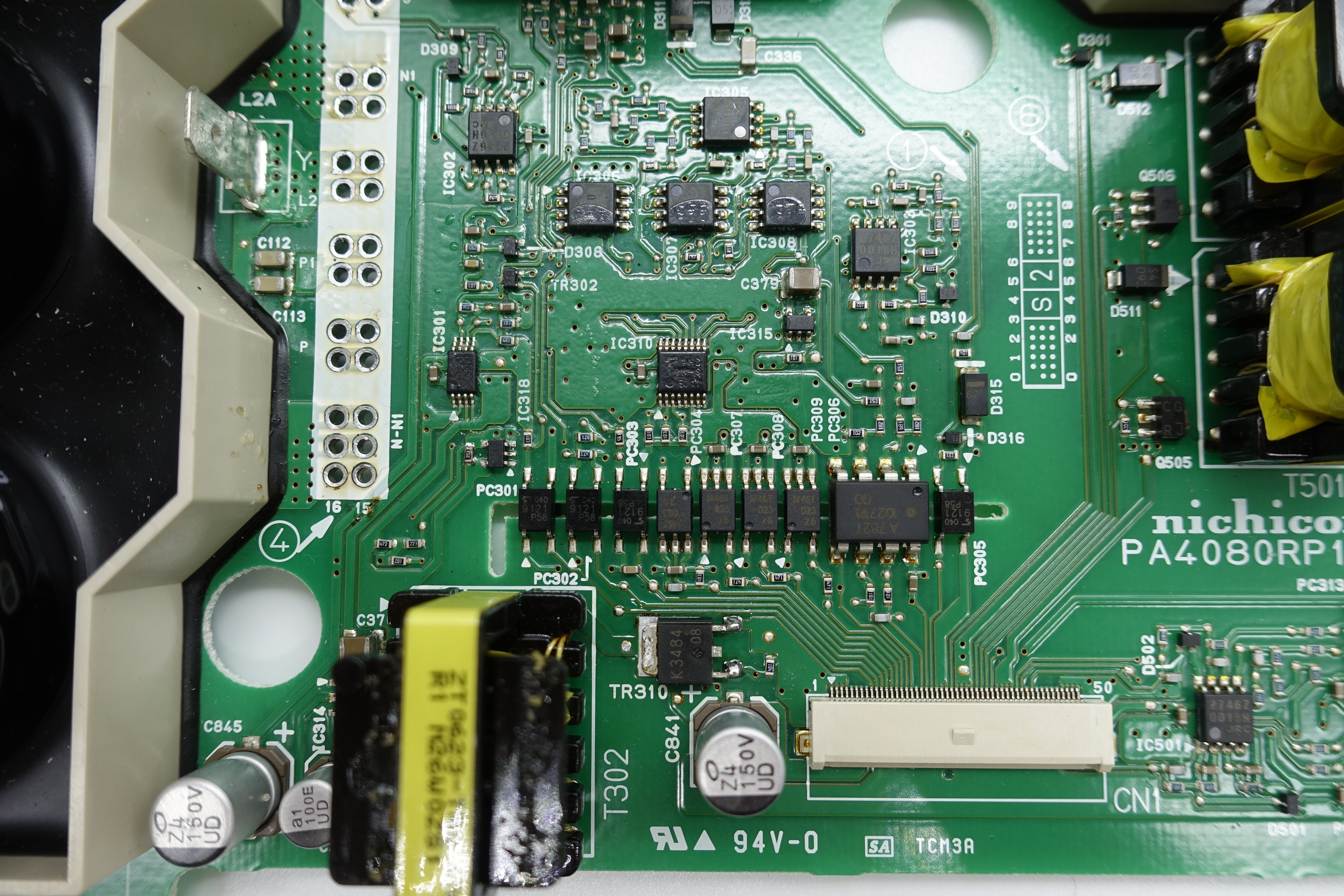
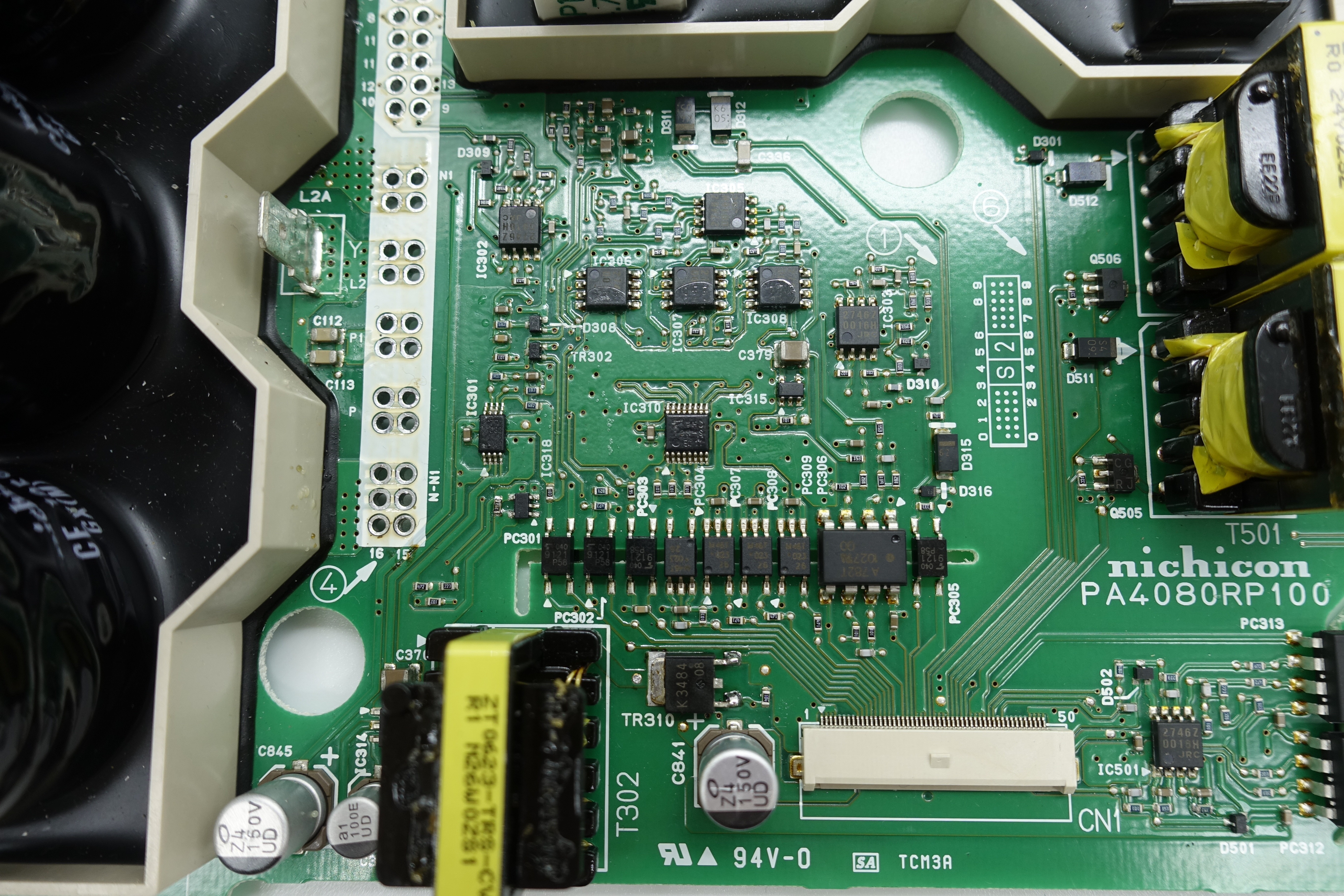
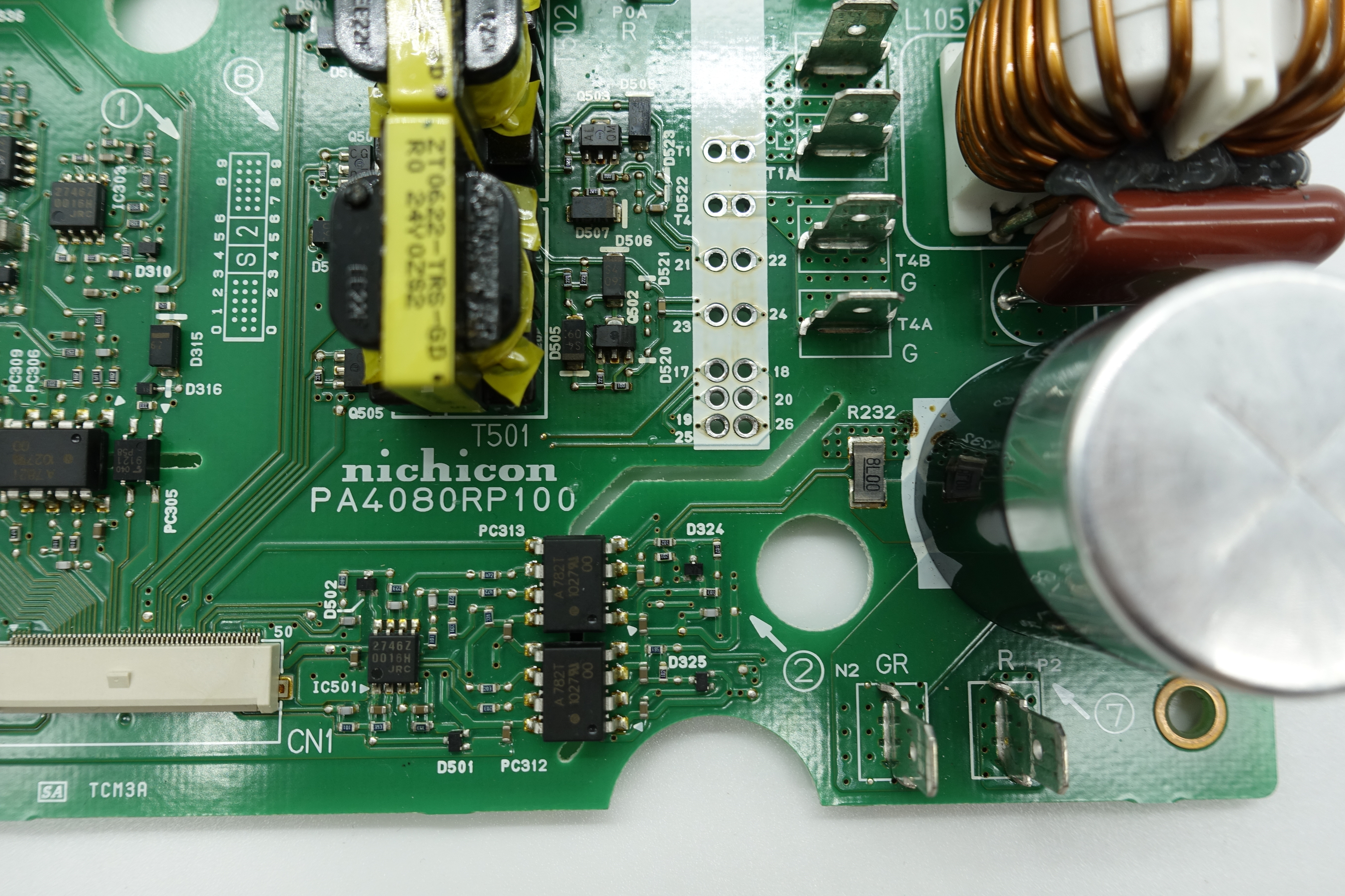
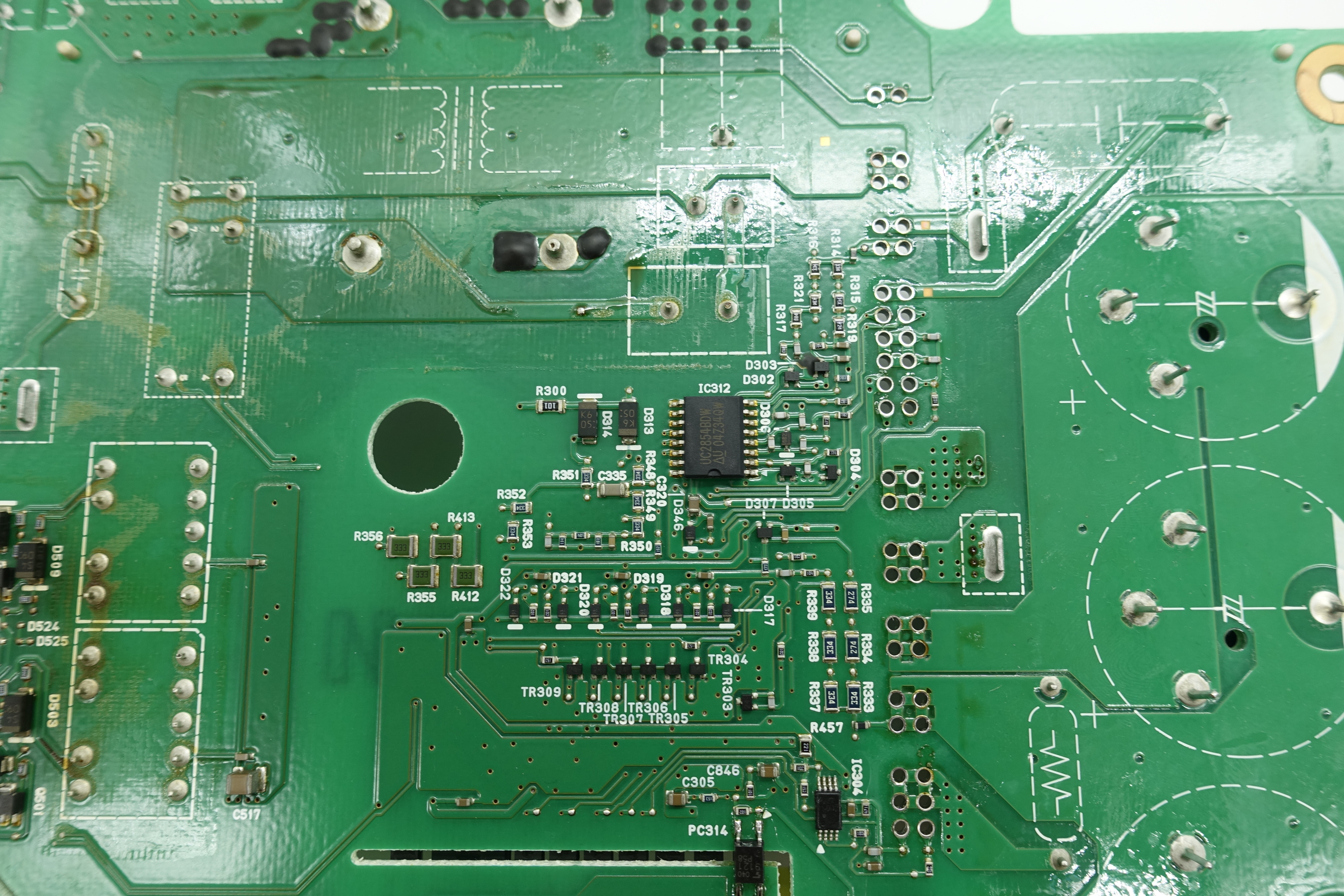
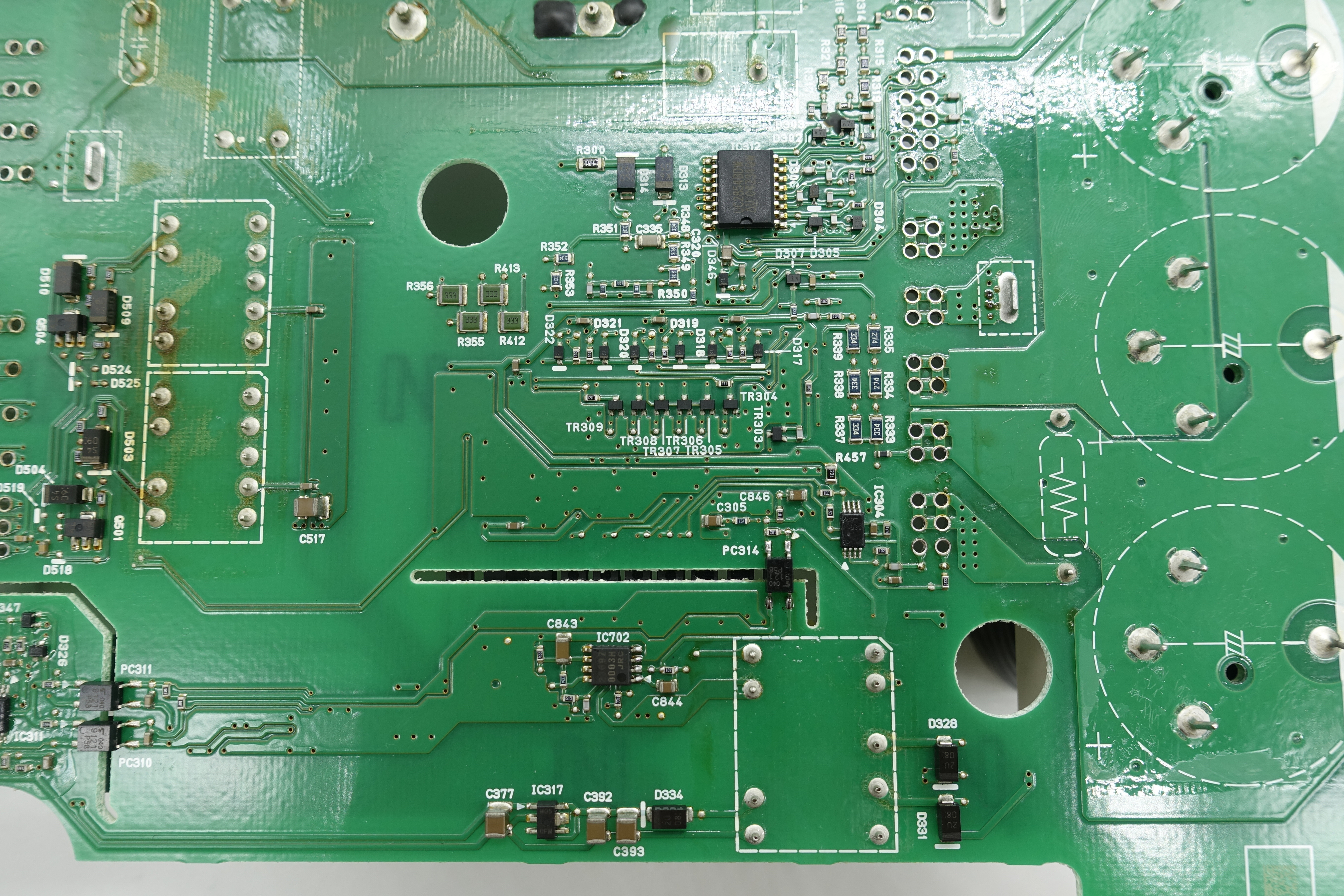
I took some high quality pictures of the board with enough light to see every trace, I hope this might be useful.

GzmEISf.jpg

u6nevTJ.jpg

7zODGiI.jpg

8jccZOH.jpg

LnXEi9t.jpg
 
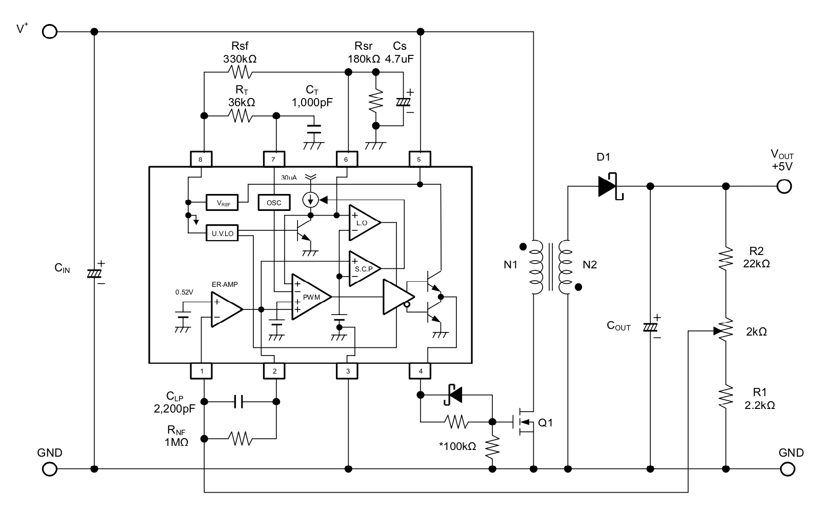
There is an oscillator for IC702 determined by an R and C on pin 7. i'm guessing that it is not oscillating for some reason, maybe it's the passive parts, or maybe it is defective. It is listed as NJM2369 for datasheet, but marked 2369Z on the chip. Here is a typical application diagram from the datasheet. This is driving the gate of TR310, so unless it is oscillating and switching, then the transformer won't get flashed, and so no secondary created.

wPID2U9.png


i'll take a picture of my trace notes and post later. If i have time this weekend i will draw it up.
 
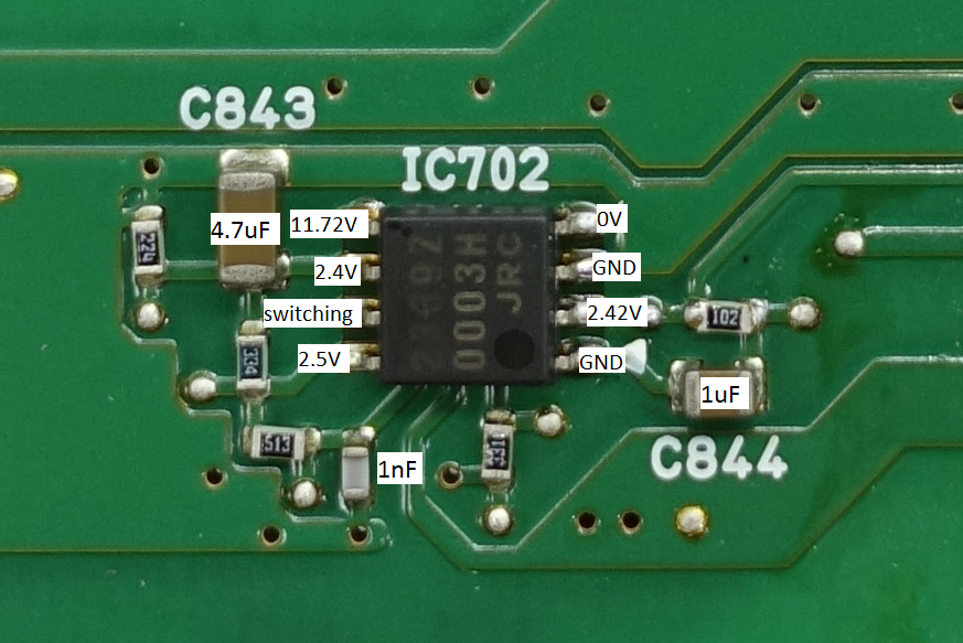
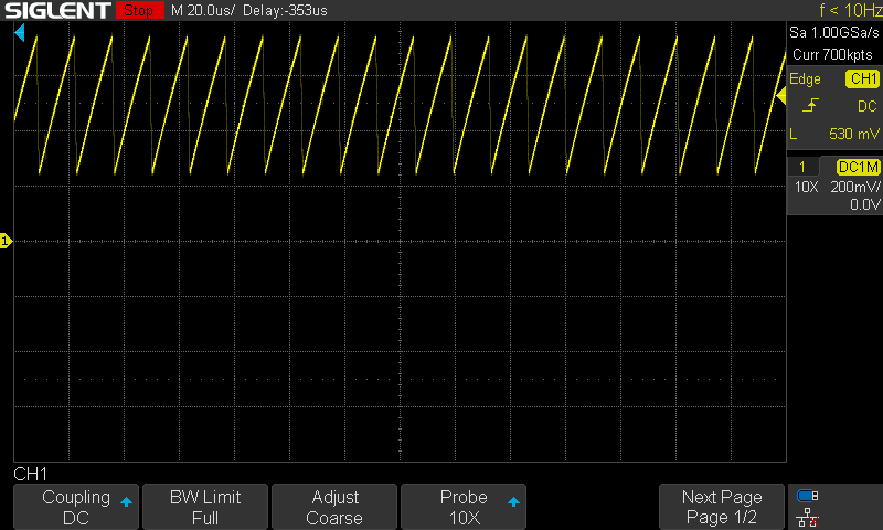
I just meaured all pins with the oscilloscope and pin 7 is switching (picture) to some degree. I also desoldered all parts seen in the picture and checked them, all resistors are fine and I added the measurement values of the caps to the picture.

oMaR5lS.png

LiMaM1J.png
 
[ Edit: this is nonsense, in light of Kenny's later post. ]

My wild guess: TR310 is shorted gate to source. If removing that transistor did not produce drive at pin 4, then the short circuit blew the upper driver transistor in IC702. Or IC702 failed all on its own. With zero volts on pin 1, IC702 should be driving the transistor as hard as possible, and it's not doing that. I'm suspicious about the low voltage on pin 2, but it's possible that this part of the circuit runs on Vref, in which case it's believable.
 
Is there a good solder joint to the ground side of the 220k resistor next to C843 ? The voltage at pin 6 CS is too high, it should be about 1 volt according to the voltage divider. This latches the chip into LockOut mode for short circuit protection, shutting off the output.

The oscillator is running about 70kHz, which is right in line with the datasheet, so that seems good.

The FB on pin 2 is at the internal rail (~2.5V) because there is no pin 1 Input, the threshold for turn ON is 0.55V on pin 1(IN). The overdrive at pin 2 also causes the PWM and Short Circuit Protection to go hi and shut off the output.

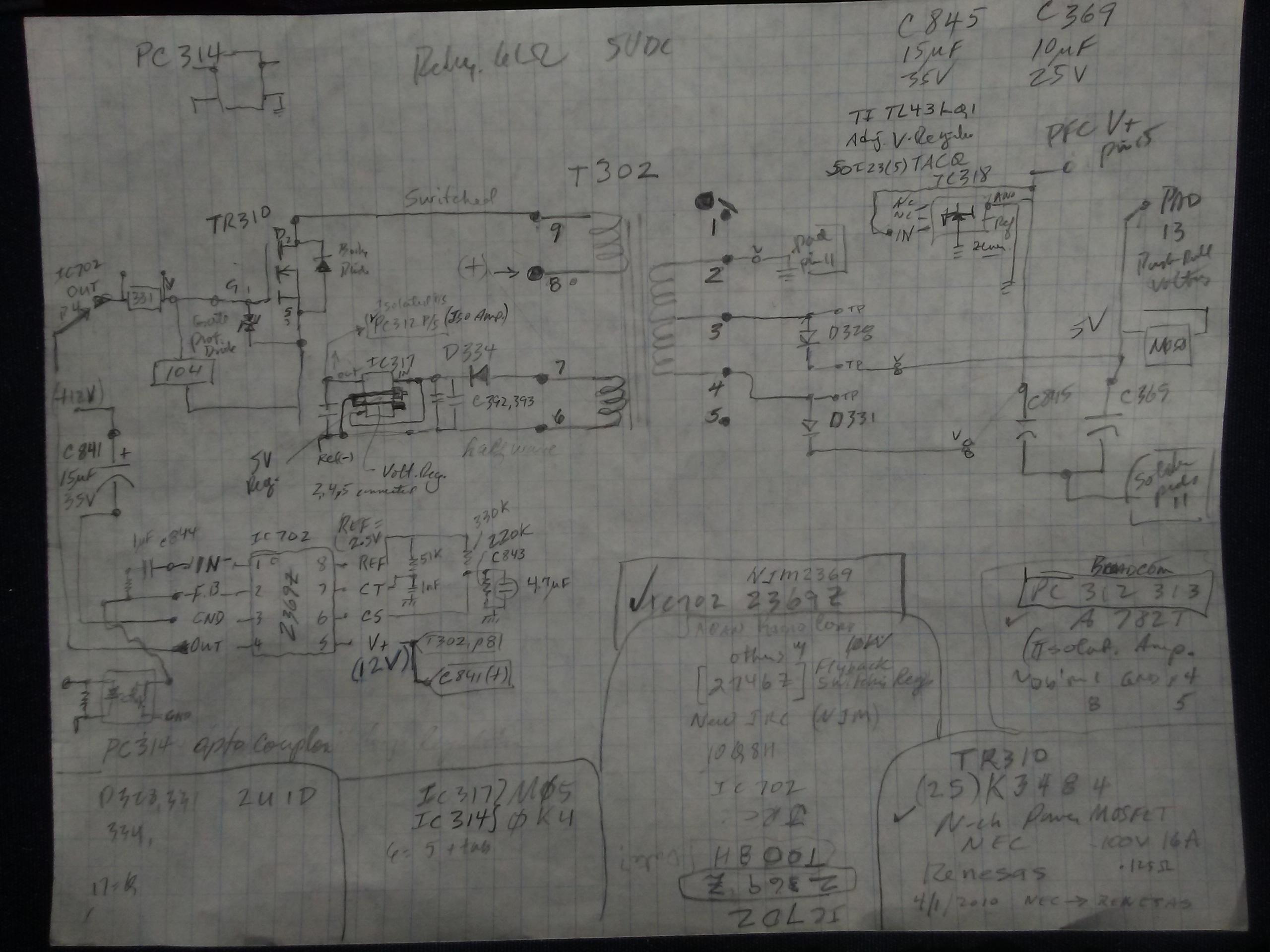
Trace notes of the transformer circuits and the feedback and Input(-) from IC318 back to IC702. Sorry they are so rough.

Z9zuk1g.jpg


DW3zIto.jpg
 
@coulomb
TR310 is fine. I desoldered the MOSFET and tested it in a test circuit and it is switching normally.

@kiev
I just double checked the voltage divider and my measurements and solder joints are okay. I resoldered the 220k resistor and removed the 330k one. Even after removing the 330k resistor I get 2.4V on pin 6. Should I remove IC702 to see of there are any vias under the chip? The voltage drop on the 330k resistor is only 0.1V. If there are not any vias under IC702, pin 6 seems to be outputting the 2.4V.

Awesome work here on your schematics! But it really seems that the 2.4V are coming from IC702.
 
There are a couple of traces under IC702, one from pin 4 to the 330R at the bottom of the picture; and one from pin 7 to the 1nF cap; and one from the fat trace at the bottom with 2 vias and a tp up to Pin 5, the 12V supply. i don't see any vias when looking from the top of the board.

The voltage on pin 6 seems to be from the internal 30uA current source, which i think gets turned on when the short circuit protection gets triggered; the external components are only pulling 11 uA across the 220k and that gives the 2.4V. This voltage is also one of the inputs to the PWM op amp.

The 2.5 volts on pin 2 seems to be the output of the error op amp due to the 0.52 internal reference on the (+) input and nothing on the inverting input from pin 1. i have an idea for a test, briefly touch a resistor (eg 100k - 1M) between pins 1 and 2 to see if it causes the chip to start switching.

The voltage on pin 2 is causing the PWM to stay locked high and also sets the short circuit protection hi which latches the chip and stops the output.

datasheet link in case you don't have it: https://www.njr.com/electronic_device/PDF/NJM2369_E.pdf
 
kiev said:
The voltage on pin 6 seems to be from the internal 30uA current source, which i think gets turned on when the short circuit protection gets triggered;
Yes. The long time constant of the Rs and C on pin 6 (≈ 0.5 sec) seems to be the short circuit protection. The logic seems to be: if there is no output for 500 ms, something is wrong, likely a short circuit (either at the IC702 output or in the transistor it drives), so best to shut it off and prevent either IC failure or meltdown of other components like the "transformer" (really a multi-winding inductor). So whenever there is a failure in this circuit, you would find it in this state: 0 V in pin 1, ≈2.5 V on pin 2, ≈2.5 V on pin 6, and no drive (0 V) on pin 4. So see the action, you need to trigger the DSO at power-up, or as Kenny suggests below, force a "reset" with a resistor or similar and capture voltages on the DSO.

The 2.5 volts on pin 2 seems to be the output of the error op amp due to the 0.52 internal reference on the (+) input and nothing on the inverting input from pin 1. i have an idea for a test, briefly touch a resistor (eg 100k - 1M) between pins 1 and 2 to see if it causes the chip to start switching.
I don't believe that will work; the short circuit protection is acting because something is wrong elsewhere. But the idea of a "reset" is good. My suggestion is put one channel of the DSO on pin 6, put the DSO in one-shot mode and trigger on that channel at about 1 V, low-going edge. Put the other channel on whatever you want to test, perhaps start with the output, pin 4. Use a clip lead or whatever to short the 4.7 μF capacitor on pin 6; this should trigger the DSO, and you should capture some 300 μs of activity. That should allow you to figure out what is happening in the initial half second before the short circuit protection kicks in. It would be best to have all the parts in place, so that you'll be able to see why no feedback gets to pin 1 (if that's the case). It might turn out for example that there is too much load on one of the "transformer" outputs (so check those as well). Pin 1 would be the next place to capture from, and work back from there.

The voltage on pin 2 is causing the PWM to stay locked high and also sets the short circuit protection hi which latches the chip and stops the output.
I believe it's the continued high voltage at pin 2 (higher than the "battery" connected to the PWM op-amp) that allows pin 6 to ramp up to higher than the rightmost "battery" that is the problem. When pin 2 occasionally goes low, it should stop the 30 μA current source from ramping up the voltage at pin 6, which should be enough to keep pin 6 low enough to stop the short circuit protection.
 
i have to agree with Mike's excellent analysis of this chip, and i like his reset method of shorting across the 4.7uF cap, that is a great idea. i was puzzled about the meaning of "CS" for pin 6 until coulomb described the logic.

The history of this circuit having failed, then working again after checking and re-soldering the passives, then failing again, is obviously an anomaly that must be solved. It's hard to know if the NJM2369 chip is defective or if some other factor is the culprit, but it would be nice to know what is failed before buying a bunch of parts.

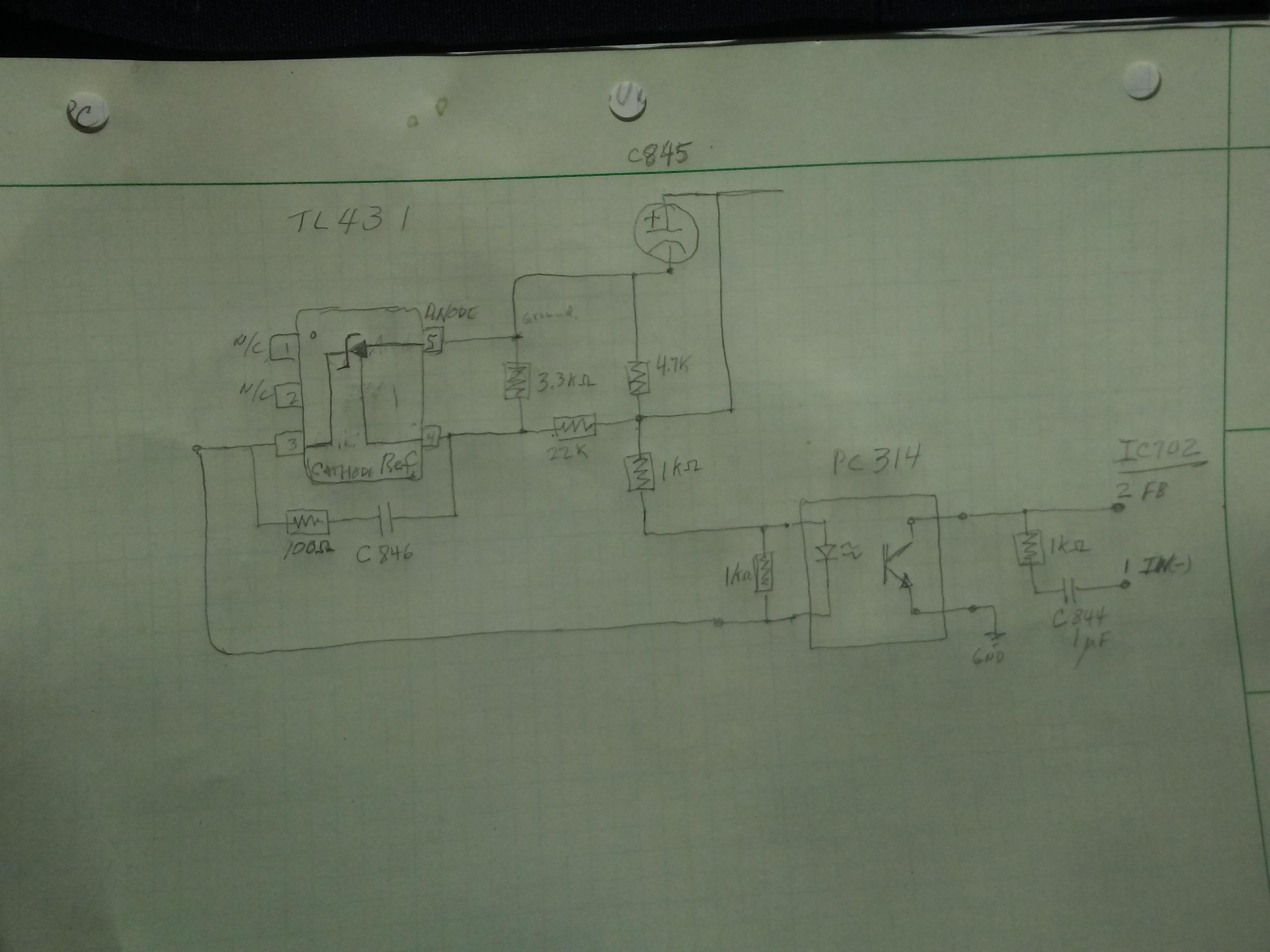
Diode D331 rectifies the secondary on pin 4 of Transformer 302 to create the ~16VDC supply stored in C845 and used by the TL431 regulator, IC318. The output of IC318 is used to turn ON the LED in PC314, TLP127, which has a darlington phototransistor output that shorts out the FB pin 2 and provides the AC input for pin 1.

Maybe the D331 or the photocoupler is not working? i measured a diode drop of 0.5 volts both directions across pins 1 and 2 for the input LED, but there is a 1k resistor in parallel. The datasheet indicates a 1.15V forward voltage for the LED. If you haven't already, then you could test it on the bench to see if the LED is turning on and the output gets shorted. Also check D331; and C845 is it defective/shorted at high frequency?
 
I find it quite odd that the feedback is applied to pin 2, and not pin 1. I mean, what is the error amplifier doing now? It's not connected to anything, except for its own feedback R and C. Maybe "FB" on pin 2 is deliberately ambiguous; it may refer to feedback for the error amplifier itself, or feedback for the whole PWM control system, if you happen to want the feedback to work in the opposite direction.

In the example schematic from the manufacturer, feedback is applied to pin 1, where too high an output will pull pin 2 low.

In the OBC circuit, too high an output will turn on the TL431, which will turn on the opto, which will pull pin 2 low directly, regardless of what happens with pin 1 and the error amplifier. The datasheet doesn't seem to suggest this as normal operation. If the error amplifier output isn't designed to be shorted low (e.g. open drain with a pull-up resistor), then it seems to me that they are using this part outside its design parameters.

I'm also wondering if I got the purpose of pin 6, "CS", wrong. Perhaps it's part of the "soft start" circuit; a time constant of around 500 ms makes sense for that too. The "C" would be for Capacitor, and the "S" for Soft Start. It's so hard to follow the internal diagram when you don't know whether inputs to a box inhibit with positive or inhibit with negative. Similarly, the UVLO (under-voltage lock-out) block outputs: are then alternatively positive? If so, which one is positive normally? Often you can guess, but it's possible to make a plausible theory that is completely wrong.

Edit: since this is the start of a new page, I'll duplicate the reference schematic from the datasheet here:

wPID2U9.png
 
Thank you so much for your effort and great details about IC702! I will try out your suggestions today and add further information to this post.

One thing that is strange is that shorting pin 1 and pin 2 with a 4.7k resistor actually makes IC702 switching again. Something has to go wrong when powering the circuit on. I just tried using another power supply and powering up both pins at different times but it seems like my test setup is right.

After powering the boards off and on again the same issue accurs but after shorting pin 1 and pin 2 with a resistor it starts working again. This is completely repeatable and I tried it for many times now.
 
@ coulomb
That is a very nebulous chip. i had the same thoughts that maybe it wasn't being used properly, but couldn't find any application notes or user guide for their regulator chips.

At first i was thinking FB was feedback, but now i'm thinking it means "Fly Back" and somehow provides information from the pulsating voltage on the secondary side.

They seem to show an input bias on the PWM, SCP and LO (lock out, or latch output?), but don't show a value--are we to assume it is the same 0.52V as used on the error amp?

@ zeta
Thanks for the update on the pin1-2 shorting test. How did you determine to use 4.7k--did higher values not work, or was that all you had handy?

Now i'm wondering if it will start if you just short pin 2 to pin 3, or pin 2 to GND (somewhere convenient to touch)?

@ all
Is it the voltage applied to pin 1 that causes the start, or the pulling down of pin 2?
[edit] found the connection of pin 1 to pin 3 later.
 
kiev said:
That is a very nebulous chip.
Indeed! And it's in a really weird circuit.

I've just realised that with the large C and small R (relative to the reference circuit) in series, there is nothing connected to pin 1 in the steady state. It's free to float anywhere! I guess there is a high value pull-down resistor to ground.

Or is there perhaps some other connection to pin 1 (perhaps through vias under the chip) that haven't been discovered yet? I'm suspicious about the opto second from the short right-angle in the slot bridged by many optos on the top side. [ Edit: Oops! I've been sucked in again by those test points that look like vias with solder in them. But of course, there is no reason for vias to have any solder in them. But I still feel that there could be some other connection to pin 1. ]

Is it the voltage applied to pin 1 that causes the start, or the pulling down of pin 2?
I think it is the voltage applied to pin 1 that causes the start. But all that does is pull pin 2 low, so pulling pin 2 low some other way would do the same thing, it seems to me.

@zetafunction, when you connect pins 1 and 2 via a 4k7 resistor, does the whole circuit work? In other words, do you then see reasonable voltages at the transformer outputs after rectifiers? I guess it would be unregulated, so best not to do this for too long.

Does it keep going after you take away the resistor? I can imagine that with the output going above and below the reference voltage, pin 1 would get pulses that might keep it running. I wonder if a 1 MΩ resistor (as in the reference circuit) would be enough? It seems crazy not to have any DC bias to the error amplifier input.
 
The 4.7k resistor works but something like 10k seems to be to high. So the 4.7k resistor is the highest value this reliably is working. When I short pin 1 and 2 absolutely nothing happens, the board starts working after removing the resistor and stays in this state.

At the time the board was magically working again, I could turn off the power and after turning the power back on it was still working. Accidentely touching the chip does not explain this behavior, so the board could really fix it self back then.

@kiev
Are pin 1 and 3 not both connected to GND? I have a resistance of 0.34 Ohm between these pins. Shorting pins 2 and 3 also results in the same behavior.

@coulomb
I am pretty sure the board is working. The voltages are looking fine to me and the current measurements match a known working board exactly.
 
did it start when pin 2 was shorted or pulled low using a resistor to ground? Or only started when the resistor connection was made from pin1 to 2?

[edit] i just measured my board and pin1 appears connected directly to pin 3 ground, i measured .1-.2 Ohms. Sorry i never checked for this before, i never expected that an INPUT line would be shorted to ground.
 
I get 0.016 Ohms between pin 1 and 3 (4 wire measurement) and I think I even traced it out a few days ago, they are both connected to GND. So I can only connect the resistor between pin 2 and GND and it starts after removing the resistor.

I also just replaced C844 with a new one from a good brand, but it did not affect the problem at all.
 
so it still has the issue of not starting until you pull down pin2? It won't start up without help after power down?

What do FB and CS look like when it's running?
 
C843 and C844 are now both new but the problem is still the same.

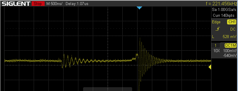
Feedback when it is running:

CW7I9jL.png

EU6jPMF.png


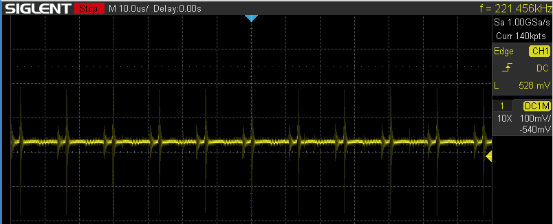
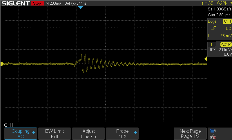
CS is at 1V but got some noise on it, I tried to capture it with AC coupling:

aPBGmvP.png
 
So FB is running at around 0.54 V or a little bit higher than the Ref. of 0.52 V. i see a 75kHz pattern to the signal, likely that is the oscillator/PWM frequency set by the RC on pin 7; then the ringing is due to the recovery overshoot after the opto triggers. The first edge ringing is ~ 8MHz, the second larger one is ~ 17 MHz.

And CS is operating at the setting of the voltage divider. The ringing ~18MHz.

What could be causing the latch up to prevent starting? The TL431 and optocoupler would seem to be okay for it to operate.

something may be shorting or pulling down the supply during startup and causes either LO or SCP to latch, then it won't start normally, then with a little help, it runs?

[edit] i can see the trace under the chip from 1-3 with a strong light and magnifier.
 
Back
Top