The Troubleshooting and Repair for On-board Charger (OBC) Thread

Mitsubishi i-MiEV Forum

Help Support Mitsubishi i-MiEV Forum:

This site may earn a commission from merchant affiliate links, including eBay, Amazon, and others.
That's good news on the waffle plate.

The boards look okay from the great pictures.

This is not the usual failure mode that we see of the snubber caps and fuse, and is probably the first time for these symptoms.

The current sense circuit was traced out, and there are some notes about the low voltage power supply, here on page 11, The transformer is T302 located on the bottom board. The 16VDC supply is located on the top board.
Output HV and Current Sense.

Not sure that the PFC was ever posted but i'll look for that also.
 
I measured out all parts involved in current sensing and they are good.

Should I inject a voltage in order to check the 5V generation and is there any point in removing the waffle plate to look at the components under it?
 
i suspect the power supplies on the top board and would recommend to look there first.

Here is discussion of the supplies, http://myimiev.com/forum/viewtopic.php?f=23&t=4079&start=70#p36876

and see page 9 for picture and skylogger's measurements. There is an always hot 12V coming into the OBC to the top board, may be able to plug that board back in and get some measurements.
 
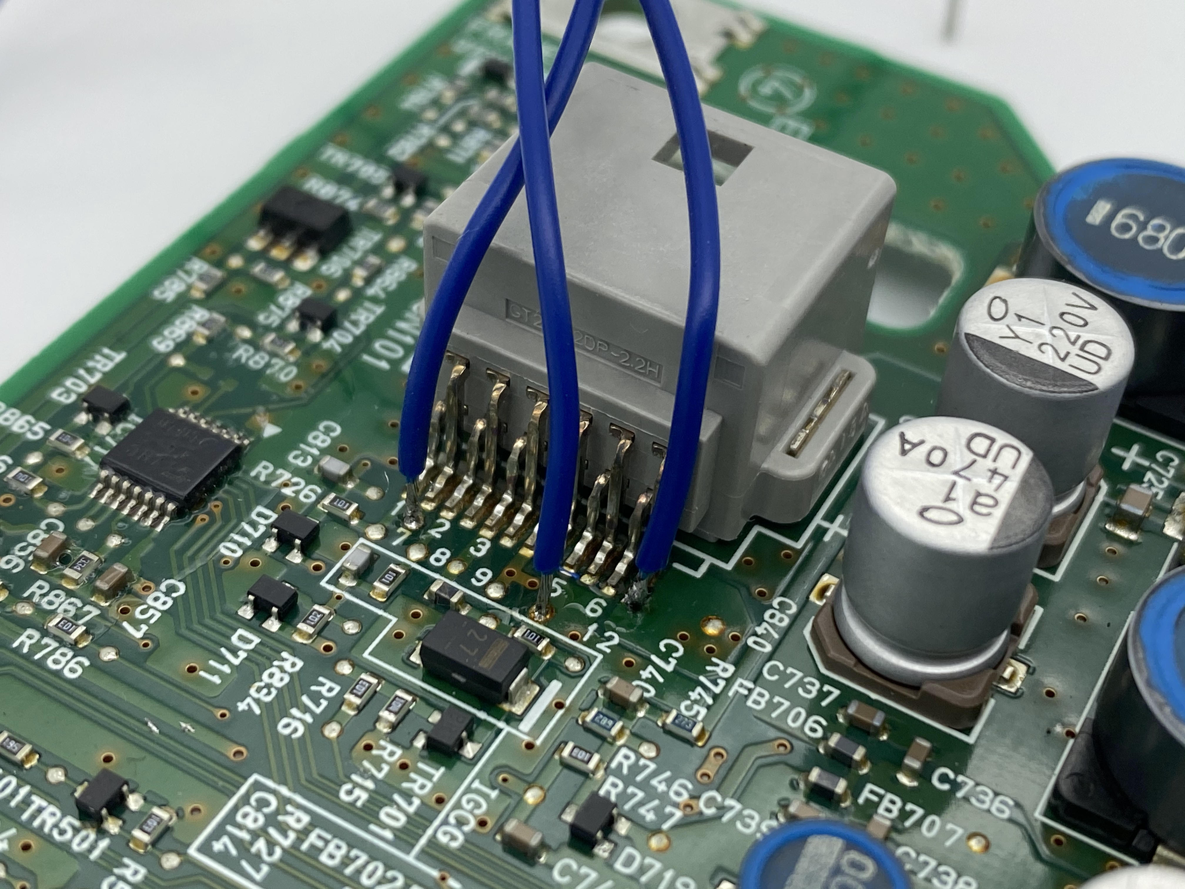
I soldered three wires to the top board to power it up and compared it to skylogger's measurements. They seem to be close enough.

12V DC with a lab bench power supply:

C702: 11.712 V
C706: 5.1322 V
C707: 16.797 V
C704: 16.8 V
C737: 5.1285 V
C701: 11.722 V

After that I noticed something. I only draw around 88.55 mA of power. Skylogger mentions a power draw of 211 mA.

I put up a picture of the wiring for further references there. Sorry for my bad soldering, but the wires are only soldered temporarily ;-)

N49DVet.jpg
 
The 16V supply gets routed thru the ribbon cable down to the bottom board and gets chopped thru Transformer T302 to create secondary power supplies for the PFC and current sense.

The current sense supply is underneath and can be seen without removing the waffle plate, regulator is ic317.

The PFC supply is held up by C845 near T302. if you connect the ribbon and power up your wiring the current may go up toward skylogger's readings due to current in the transformer. The PFC ic is a TI UC2854BDW and i traced the Vcc pin 15 back to the + on C845. It looks familiar like i've traced it out, but i'm not finding my notes.

i'm hoping there is a supply issue; it's hard to believe 2 separate circuits could fail at same time unless something common, e.g. supplies feed off of T302 secondaries.
 
I just checked this circuit and there is a problem there. There is no voltage across C845 present! The voltage enters with about 12 V the connector and gets to TR310. Between the drain of TR310 and the connector ground are still 12V.

Is it possible, that T302 is the problem?
 
kiev said:
OBC 39 is Power factor correction (PFC) circuit output voltage abnormal; the PFC boost is done after the rectification of the input AC voltage and is in the vicinity of the 3 large capacitors on the bottom board. The control ic IC312 for the PFC is on the bottom side of the board, so i would recommend to check all the diode drops in the waffle plate first to rule out a major semiconductor failure.
OBC fault code 39 is also set and charging fails if the AC input voltage is too high. (voltage "abnormal") I have had this happen to me.

Before going too much further I would measure the AC supply voltage at the time the charging failure occurs. Do not believe the AC voltage reported by Canion - it has considerable error. Measure with a multimeter on the same or nearby circuit.

On my Ion the car would refuse to charge and set OBC 39 above 246 volts AC ! In the UK it is allowed for the AC voltage to be as high as 252 volts and still be in spec....
 
zetafunction said:
I just checked this circuit and there is a problem there. There is no voltage across C845 present! The voltage enters with about 12 V the connector and gets to TR310. Between the drain of TR310 and the connector ground are still 12V.

Is it possible, that T302 is the problem?
i suppose the transformer could be bad, but more likely something in the chopper driver and feedback circuit. i'm going to paste this as reference from a post on page 8:

There is a DC supply voltage coming from the Top Board across the CN1 connector on pins 5-8, with ground on 1-4 and 47-50. This is filtered by an electrolytic cap, C841, 15uF 35V, and is then chopped thru a transistor TR310, an N-FET 2SK3484 100V 16A, to excite the PRIMARY on pins 8-9 of the CV transformer, T302. The gate is driven by a 10W flyback switching regulator chip, IC702 JRC 2369Z.

There is a First Secondary on T302 pins 6-7 that is half-waved thru diode D334, 2U 1D, that ties back to the CN1 supply ground and regulated by IC317, M050 5V regulator. This 5vdc is used for the supply voltage on two isolation amplifiers, PC312, 313, Broadcom A 7827. PC313 is sending the output current sensed thru R232, 0.008 Ohms, across the isolation slot to an op amp, and then on to the CN1 connector back to the top board. PC312 is sensing the [edit] HV output voltage and sending it back up to the top board on CN1, pin 42. So the box is smart enough to measure itself and likely won't come on if something doesn't feed back properly to the top board.

There is a Second secondary winding on pins 2-3 that is half-waved thru D328 2U 1D, filtered by C367 10uF 25V, regulated thru IC314, M050, that creates another 5vdc routed to IC301, etched part number ?277?.

And there is a Third secondary winding on pins 2-4 is half-waved thru D331, filtered by C 845 15uF 35V, that provides ~ 16.6 vdc supply voltage for the PFC chip, IC312 UC2854 and to the solder pad pin “13”, which is the positive rail of the push-pull gate driver for the 3 PFC gates. There appears to be an adjustable shunt regulator at IC318, marked TACQ, TI TL431-Q1, that provides a feedback signal back to the flyback regulator chip, IC702, that is pulsing the transformer. The 16.6 was my calculated value based upon the resistor network for the shunt regulator.

The ground reference for the 2nd and 3rd secondaries is to solder pad “11”.

ic702 is located on the bottom side at the edge covered by the waffle plate, but it sends the gate drive signal to the TR301 FET based upon feedback from ic 318 (very tiny and located near PC301) to excite the PRIMARY winding of TR302.

If it is not working properly then the 3 Secondaries will not be energized and you would not get any of these low voltage dc supplies. i.e.. the rail for the PFC push-pull, and the current sense 5V supply.

i would first probe to check anything you can reach such resistors, chip capacitors, diodes, etc.

Does TR301 have a body diode internally, that could be checked.

There is a 330 Ohm resistor from pin 4 of ic702 to the gate of TR301. It has test point solder blobs on each end that you might be able to reach. Maybe it is open circuit?
 
OBC fault code 39 is also set and charging fails if the AC input voltage is too high. (voltage "abnormal") I have had this happen to me.

Before going too much further I would measure the AC supply voltage at the time the charging failure occurs. Do not believe the AC voltage reported by Canion - it has considerable error. Measure with a multimeter on the same or nearby circuit.

On my Ion the car would refuse to charge and set OBC 39 above 246 volts AC ! In the UK it is allowed for the AC voltage to be as high as 252 volts and still be in spec....

I just checked the voltage and it is not above 246 VAC.

Does TR301 have a body diode internally, that could be checked.
I can measure the diode and it seems to be working.

While powered up I can measure a voltage drop of 11.754V between the source and the drain of TR310.

Across Pin 5 and 8 of PC312 and PC313 is a voltage of around 5.2V while I can not measure anything between Pin 1 and 4.

My total power consumption is 125.87 mA, still below skyloggers measurements.
 
skylogger was measuring the same ~12V across the FET with a voltmeter and used a scope to see it actually chopping.

But your reading on the PC312, an A782T isolation amplifier with separate power supplies on the input and output stages, indicates that the supply for Vdd1 at pin 1 is not being created, and that would be coming from the chopper action of the FET.

Maybe you can use AC function on meter to read for any voltage on pins 6-7 of the transformer? That would be a clue if FET is working and where to look for cause. e.g D334, ic317, D328, D331 on bottom.

It seems like you are close to finding the culprit.
 
So first of all, thank you for your patience and the great support you are giving me! That helps me a lot.

I have two multimeters here and they both measure a frequency of around 130 Hz between Pin 6 and 7 of TR301. But this reading is not stable at all and they both show 0V. I think the MOSFET might not be chopping, but I can not confirm this without a proper scope which I dont have at the moment.

I checked every part I could reach and measure in circuit on the bottom with the power turned off. Is there any way, I can check IC317?
 
i have to run right now, but i think this is it:

NCP4641 is a CMOS 150 mA linear voltage regulator with high input voltage and ultra−low supply current.
 
The IC317 does only get 0.6 V as input voltage. This results in a 0 V output. I do not think that IC317 has shorted out, but I can easally desolder it to try, if you think that happened. I also noticed that after I connect my supply, the voltage is around 1V and then slowly decreases to 0.6 V
 
That is not likely the problem-- it is not getting any voltage thru the transformer and your test just verified it from another direction. you could test it on the board with a current limited power supply, just put 6 volts on the input and should see 5 on the output, but

IC702 (on bottom side) provides the gate drive for the FET, so it is likely not doing it's job. And IC318 (on upper side) provides the feedback signal to ic702, so it will be one or the other of those two chips, or some little passive component in those circuits, resistor, cap, diode, etc. There may be discussion of this on page 9. If i get time i will try to trace it out and draw it up better than the hand sketch, but i have some medical appts tomorrow and will be off line most of the day.
 
There is also an optocoupler pc 314 on the bottom side that sends the signal from ic318 over to the gate driver ic702, but the waffle plate probably covers it from probing. Several small resistors on top side near corner of transformer are the voltage divider for ic318.
 
Today I bought myself a scope and I can conform that the MOSFET is not chopping at all. Everything around IC318 looks fine to me and all components on the bottom side are covered by the plate. Even if I could reach them for probing I would not be able to replace them. So I think I have to desolder the plate.

Should I buy a desoldering station with an integrated vacuum pump for this job or how would you desolder it?
 
That's what i used. Some of the junctions have wide copper traces and a big thermal mass, and i damaged a few by pulling and forcing them out while there was still too much solder down in the hole.

i would have done better to add some flux to those pins, then a hot iron and try to draw the solder up toward the top with wick or wire if necessary and make sure the holes were clean. Add solder to a joint to increase the thermal mass and capillary action sometimes works.

or use a hot iron and wooden chop stick to repeatedly heat-and-pry, heat the pins and pry up the board from underneath to walk the board up the pins and use wick to clean up the holes once its off the plate and on the bench.
 
Thank you so much for your time and effort! I just ordered a desoldering station which will be delivered in three weeks. (I ordered a JBC one and JBC stuff takes forever to ship to me) As soon as I get it I will be posting my progress here.

I will in addition to your suggestions add leaded solder in order to decrease the melting temperature and preheat the PCB to 80°C
i would have done better to add some flux to those pins, then a hot iron and try to draw the solder up toward the top with wick or wire if necessary and make sure the holes were clean. Add solder to a joint to increase the thermal mass and capillary action sometimes works.
 
Might as well try to order some new parts while you wait, the ic318 and ic702, maybe even the FET, TR310, unless you are sure it is good. But why not fresh it all up while you are in there, you don't want to have to go back in there again.
 
After waiting several weeks for my desoldering iron I finally got rid of the waffle plate. All components around IC702 measure out fine to me and assuming IC702 is a TI OPA2369 I can measure 2.4V between V+ and V-. How could I check, if this IC is working or would you recommend looking at something else instead?
 
Back
Top