Gen1 DCDC Converter Troubleshooting and Repair

Mitsubishi i-MiEV Forum

Help Support Mitsubishi i-MiEV Forum:

This site may earn a commission from merchant affiliate links, including eBay, Amazon, and others.
eldenh said:
... I mounted the board with the 4 screws that have metal pads assuming them to be important, but have omitted #s 4, 6, 7 expecting to have to remove the board to replace whatever had failed.

Trying to troubleshoot from your pencil sketches has been rather difficult because my eyes have trouble distinguishing the pencil lines from a grayish background. I choose to build a spreadsheet to help me find where I can try to probe with the board mounted. In doing so I found that Q219 is listed as "KN" and "G16". I can't make out the label in the underside photo, so don't know which is right.

That's excellent to recognize those screw pads; was there a good solid connection to the 12V negative, not just thru the little ground wire on pin 5 of CN201?

Good catch on the list i had it twice; on my board Q219 is "G16" N-fet IRL2502, and Q218 is "KN" P-fet 2SJ305.
 
It has never been clear to me if you were testing in the car or on a work bench, so that is why i mentioned the need for a good ground for the board. The 4 screw pads are not connected to pin 5.

All the return current for charging the 12V aux has to return back to this board thru the housing. The Pin 5 wire is not the path we would want it to take, e.g charging at 60 Amps.

One is a signal ground, the other a power ground. Ultimately they are tied to the same reference level, but damage will occur if the power ground uses the signal ground as a return path.
 
I've been using the chassis for LV ground when testing. I've been testing on the bench as I don't think I can make connection in the car and safely reach the dc-dc converter.
 
I measured the voltage on all the pins of IC202: 1 is 0v, 2 is 0v, 3 is 15.5v, 4 is 4.66v, 5 is 0.17v, 6 is 2.27v, 7 is 0.15v, 8 is 1.63v, 9 is 0.10v, 10 is 3.26v, 11 is 0.08v, 12 is 0v, 13 is 0v, 14 is 0v. Pins 4/5 surprise me as the data sheet gives max differential voltage as 3.6v! R256 has 15.5v and 4.66v, R251 has 0.02 and 0.0v, R250 has 2.27 and 0.02v, R249 has 2.27 and 2.42v, and R248 has 4.66 and 2.42v.
 
That was a good test. You can measure the response at the collector of Q223 and what pin 12 of IC207 (both on the bottom layer) are seeing from the top, there is a tiny trace coming out from under the CN201 connector on the side opposite of the CN201 label, this trace terminates into a little double via with the tiny holes. This point is the line shown on the schematic on Q223. That pin should change state depending upon presence or absence of the Output 12V battery connection.

The logic would be that the PWM would not start unless there is a 12V on the output side, so when Output 12V is present then the double via should read Hi, when no 12V it will go Lo.

Just saw you measurements on IC202, it is a quad comparator but i don't have but the -A,-B or -D of the quad traced yet, only the -C circuit. But all the output readings are consistent with the input voltages.
 
[ Edit: The below is all wrong. I was confusing IC201 and IC202. Sigh. Sorry for the confusion. ]

eldenh said:
I measured the voltage on all the pins of IC202: 1 is 0v, 2 is 0v...
0 V on pin 2 is bad; according to Kenny's traced schematic, it should be +5 V. Perhaps it connects to Vref, pin 16? You didn't give a voltage for pins 15 (Vcc) or 16 (Vref). I assume that Vcc must be 15.5 V or slightly above, for pin 3 to have 15.5 V.

Pins 4 and 5 are the oscillator. The oscillator could be stopped due to pin 8 (soft start) being low, though above 0.2 V it should be soft starting. It's not clear to me whether you need to keep pulsing pin 8 low to get more than one pulse from the output; I suspect that you do. In normal operation, pin 8 should be above 5.0 V.

Actually, if the block diagram is accurate, the oscillator should keep going, and other parts of the circuit should keep the output low despite the oscillator running. So it may be that there is a problem with the oscillator parts. There are probably only 2-3 parts connected to pins 4 and 5.
 
Mike, I think you are confused about IC202. It is a 14 pin quad comparator device with V+ on pin 3 and V- on pin 12. It is located near the double large capacitors by the output fuse.
 
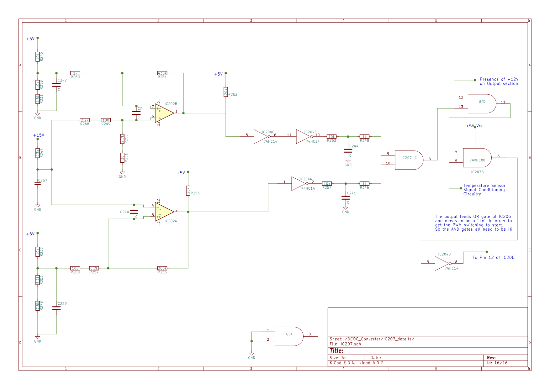
Here are the last two AND gates [from the IC202-A -B comparators] that affect the signal to the IC206 OR gate pin 12. These could be stopping the PWM if the OR gate is Hi.

So that one OR gate on pin 12 is a combination of 3 conditions: the temperature sensor, the 12V on output, and the level of the TP201 secondary supply voltage nominally "15V".
IBeg39R.png
 
i don't know how you knew to check the voltages of IC202, but that was a stroke of genius and it seems to be a direct hit on what is causing your problem.

There are 4 comparators that set a threshold voltage on the + pin and compare it to a signal on the - pin. Two of these use the TP201 voltage (shown as 15V but it can vary depending upon the HV Input and the operation of IC101 as it is the low-side secondary of TR105) as the input signal, the other two use the 12V Output voltage as the signal.

The 5V supply is used to set the threshold and for the pullup on the open collector output. A positive feedback resistor is added to create hysteresis filtering to prevent ringing or oscillation in the output signal when passing thru the threshold level.

In your measurements of IC202 all of the + pin input voltages are nearly zero, meaning that either the 15V TP201 and 12V Output voltages are too high (exceeding the threshold level), or that the 5V supply is not reaching that area of the board and creating the threshold voltage of the resistor divider networks, or that the chip is just bad.

The 5V voltage divider networks for the Threshold (Non-inverting inputs pins 5 and 7) seem like the 5V is missing. The 5V is available to measure on the top layer as double vias with the larger diameter holes, one is near C236 on the end of IC202, the other between IC205 and the edge of the board near R245. The 15V double via is close to the second 5V also.

One counterpoint to my bad chip theory is that you measured a response when disconnecting the 12V from the Output, so at least that seems to indicate correct operation of the comparator on those pins. But there still could be a defective 5V.
 
Thanks for the research and explanations. I found only 0.28v at both of those vias. But I've now created a larger problem. My probing created an arc around Q110 and blew R129 off the board and I believe Q110 has failed and some of the copper is melted. I can't read any value for the loose resistor either visually or with my vom. R128 is only partially readable and I am having trouble getting a measurement.
 
Oh no, can you explain where and how you were probing when this occurred? Q110 is in the HV section and i don't understand how that would be affected by probing in the LV section?

R128 has a value of 100Ω and is a "0603" smd size.

R129 has a value of 1.5Ω and is a "1206" smd size.
 
I was checking around to verify that my batteries were supplying enough voltage to have a working board. When I tested Vsub I read 0 and probed the terminals of Q110 to see why. I'd forgotten that I should be checking with my other probe on the HV neutral. :oops:
 
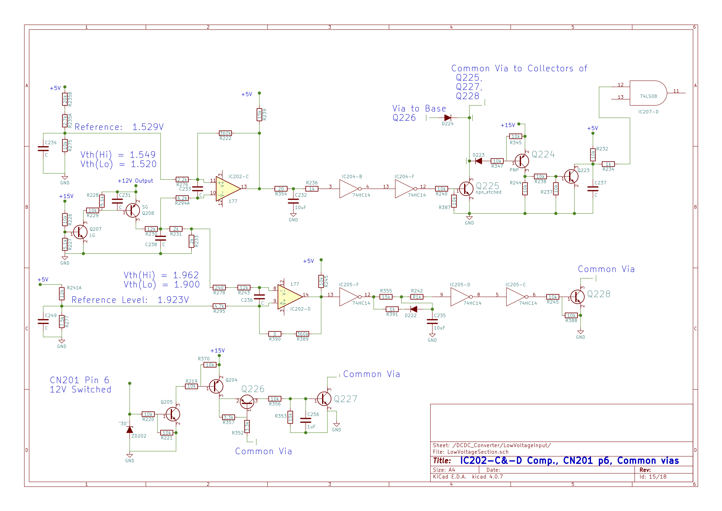
i didn't like how the drawing was folded around on the IC202-C Comparator section and it was incomplete;
[edit] added additional findings
traced out the -D Comparator path;
found a linkage to CN201 pin 6 to the control function and the Common Vias on the transistors.
piJqyfM.png
 
I find it difficult to read the resistor values in the drawings, so I want to ask for an explanation of the functional properties of the comparator and signal processing of their outputs. It looks like A & B sections determine that a 5v power ail is between certain limits and there is feedback around the comparators to provide different levels to switch back. Sections C & D function similarly for the 12v output line with Q223-225 being used to verify the presence of 15v and 5v power. Does this upper limit serve to switch off IC201 when the output line reaches it's intended max voltage {14.4v}? I had assumed that that limit was controlled by voltage feedback to IC201.

Where is the 5v that sections A & B are monitoring derived?
 
The 5V is made on the bottom layer, IC209, from the "15V" of the secondary seen at TP201 with respect to chassis ground.

Are the resistor values blurry or too small or what is the problem? The schematics are image files that you can right click and save to your device, then use an image viewer and zoom in if necessary.

i will repost the last schematic with notes about the switching threshold voltage levels.

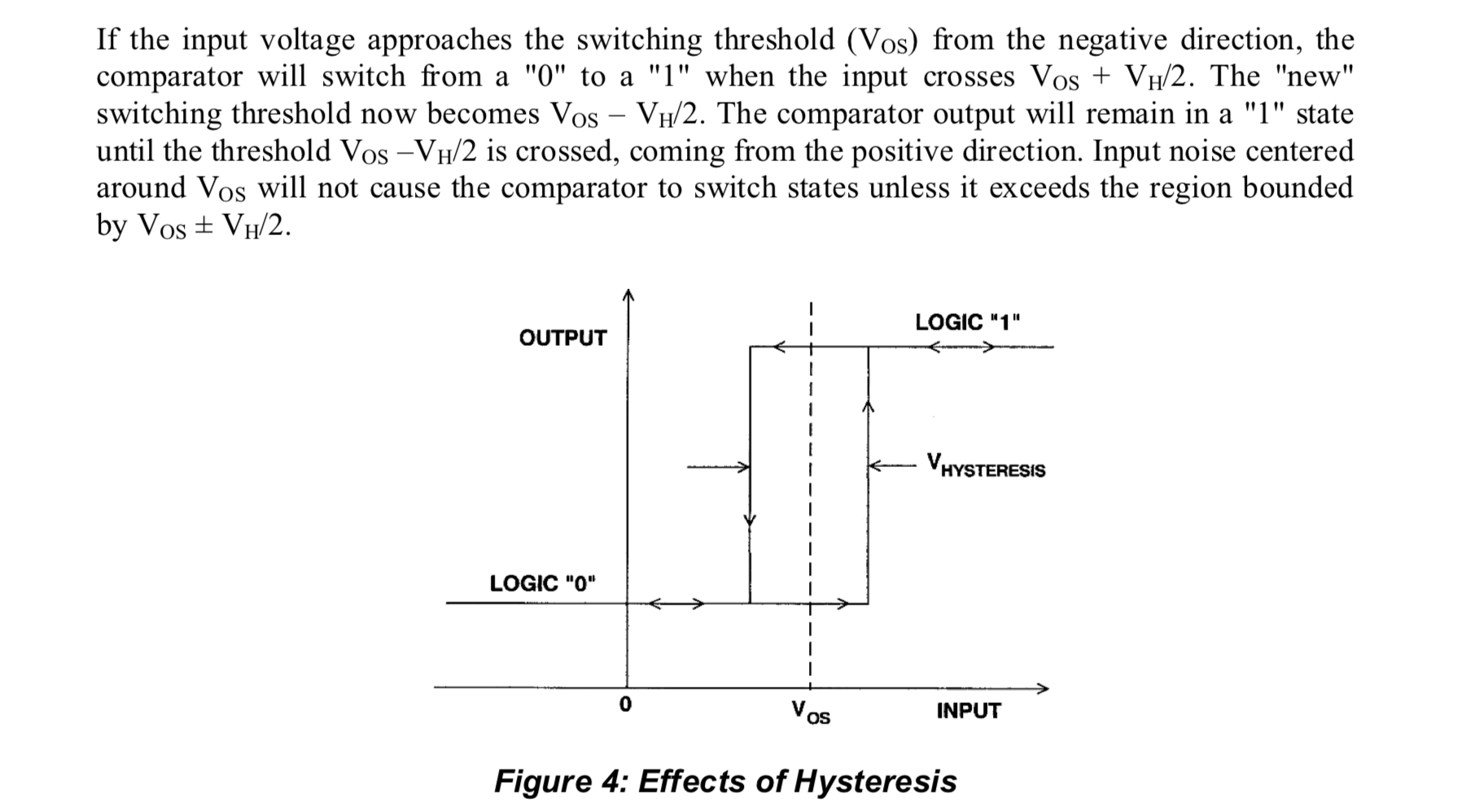
The set point reference is developed from the 5V and the feedback resistor from the output to the + terminal causes a hysteresis action to filter out oscillation as the signal passes thru the set point on the way up and back down. When the signal matches or exceeds the V Threshold(Hi) it switches output to the Hi state; Then when the signal is headed back lower than the low Threshold, the output switches to the Lo state.

ref from application notes
mN8vWn1.png


For the -C and -D comparators, the "Signal" is level of the Output 12V to decide something; the -A and -B are looking at the TP201 "15V" supply as the "Signal" to decide when to do something. There will be a certain time delay as the secondary voltage is coming up; the comparator outputs can be used to regulate or turn something on or off based upon the voltage level of the "15V". i don't know what all that is yet, there is still a lot of stuff to sort thru in that LV section.

The -C leg is what was traced earlier in crude form to determine that it was one of the causes for the PWM to start or not by commanding pin 8 of IC201. Both Pins 8 or 9 of IC201 can be used turn off or restart the PWM switching.
 
Back
Top