Gen1 DCDC Converter Troubleshooting and Repair

Mitsubishi i-MiEV Forum

Help Support Mitsubishi i-MiEV Forum:

This site may earn a commission from merchant affiliate links, including eBay, Amazon, and others.
It dawned on me that I can arrange a higher HV voltage source with my mower 120v batteries. I remounted the board and hooked two batteries in series producing 226v. When I hooked it up, Vsub measured 20.7v and TP201 15.6v. TP202 and TP203 are 0.12v and I measured 0v at the LV output. Pin 8 of IC201 is 0v.
 
Well that is some great progress.

The voltage on Vsub with respect to HV(-) or "N", and TP201with respect to chassis ground, means that the TR105 HV section is all working and creating the secondary power supplies stored on C122 and C212. So no problems there.

The other measurements make sense in that the PWM chip was not commanded to start and wasn't switching, due to no "load" for the output. Which is to say that it's not clear whether you had the positive terminal of a 12V aux battery connected to the output with a good path to chassis ground of the DCDC?

If not then a 12V aux battery would need to be connected to the LV output in order to sense the voltage for the regulation. The negative terminal would connect to the chassis ground point.

But Before doing a loaded test, if you could carefully measure the voltage on pin 16 with respect to chassis ground of IC201 in the same setup that you used in the reported test--it should read 5.1V, Also if possible very carefully not to short any pins, read voltage on pin 7 wrt chassis ground, expecting to see about 1.6 to 1.7 V with no PWM switching. If these don't read, then don't proceed.

Also what signals were applied to the CN201 connector? i don't know what the voltage level of the DCSW signal should be, if it a 5V level or 3.3V? All the ICs in the LV section are 5V, but i know lot of circuits in the EV-ECU are 3.3V. Maybe test it with 3.3V on pin 1 first to see what happens. If this is all manual testing then nothing is needed on the SDW pin.

Without cooling then only momentary operation while loaded--have the meter connected to measure the output voltage before making the connection on pin 1 and make provision to remove the pin 1 signal to shut it off quickly.

i think i sent you my home email in a PM, feel free to use that if you have questions.
 
It took a while to get the connections thru E03 to be stable! It doesn't respond with 3v on the white wire, so I tried 4.5v and still no response. I checked at pin 8 of IC201 and found 0v. At CN201 the white wire is 4.2v. I can't seem to trace the connection between pin8 of the IC and pin 1 of CN201. The voltage at TP202 & 203 did not change.
 
What about the pin 16 and pin 7 voltage readings on IC201?

The path from pin 1 CN201 to pin 8 of IC201 is not direct--there are a couple of transistors and logic gates in the path, Q234, IC206 pins 13 thru 8, and Q203.

This manual testing that i am talking about is using CN201 only to test the board, so i don't understand the E-03. Is this in the car or on the bench? How about a picture of your setup?

What is your level of knowledge, skills and abilities with electronics? Are my messages too technical or too simple for your level of understanding?
 
eldenh said:
Pin 16 is 5.07v. Pin 7 is 1.61v.

Thank you for that. This gives me an indication that the precision 5V regulator is working and the IC201 is getting the necessary power to operate. So that rules out some additional sections of the board as being the culprit,

If all the diodes and transistors in the "200" section from IC201 over to the 4 big FETs were checking okay with no shorts or damage, then the issue is likely in the section around CN201 on the LV side of the isolation gap. i've only traced about half of all those circuits and not enough to understand the logic and feedback.

So here is another check, put your HV on the P and N, and connect the two 12V and ground to the CN201, then measure the voltage on Pin 13 of IC206. Then put 5V on CN201 pin 1 and repeat the measurement.

Should be 5V the first time and nearly ground the second.
 
I found 0.12v for both conditions. I've found that the voltage from pin 1 of CN201 drops to 0.7v across R274 and there is 0.7v on the base of Q234 and 0 on the other two terminals.
 
Those readings are pointing to an issue on the 5V Vcc, or coating on the board blocking the readings.

The collector of Q234 with the 2 tiny vias, should be reading 5V with no DCSW signal on pin 1. There is a Zener diode ZD303 on pin 1 to ground marked "30", i would guess that is a 3.0V zener to limit the input voltage. i measure a 0.7V diode drop in the forward direction and about 2V in the other due to the parallel resistors across the zener.

The base of Q234 should read about 1/2 of whatever voltage is put onto pin 1 up to about 6 volts, then it should read 1.5 [half of the 3.0V zener voltage] for anything higher than 6, e.g. 7 or 8 will still read 1.5 at the base.

What do you measure on pin 14 of IC206? Should be 5V Vcc.

Also what about the voltage on Pin 9? Should be around 0.17V.

There is a thick clear coat on all the components that can cause errors in readings; i spend about half my time just peeling that stuff off of everything so i can get good traces.
 
There may be a problem with the PWM chip or the components around pin 8 of IC201.

Pin 8 should gradually charge up to 5V when the chip gets power, by an internal current source that feeds out into C226. i measure about 3 to 6 MegOhms across that capacitor from both directions. If that cap is shorted or transistor Q203 is shorted, then the pin 8 voltage would be getting pulled low and not let it get charged up.

So those parts need to be checked.

There is a latch up condition that could be an issue, and also just an issue of a bad chip and the internal current source is bad. i need to study up on that chip to know what is likely.

Here is the info from the datasheet:
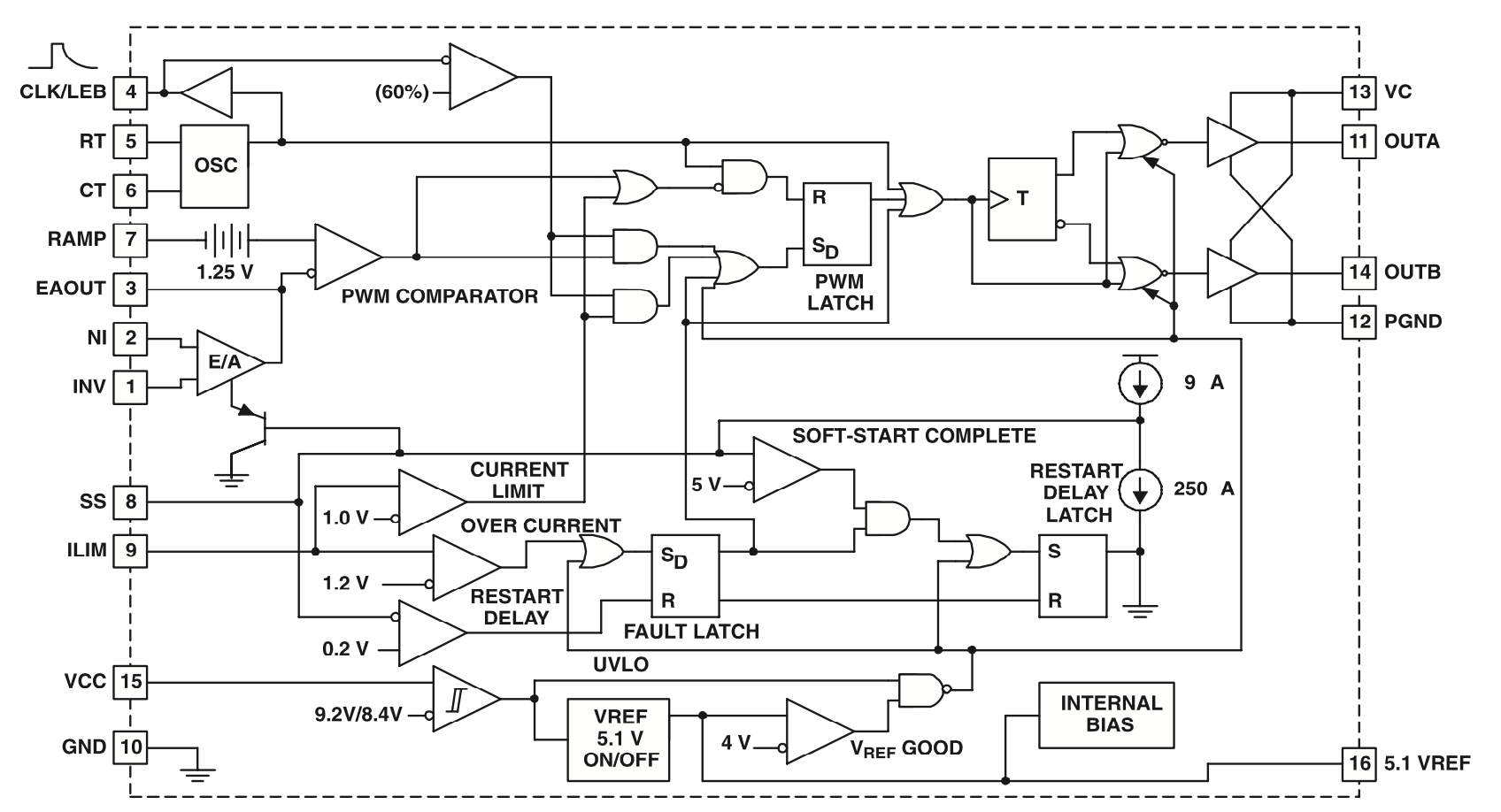
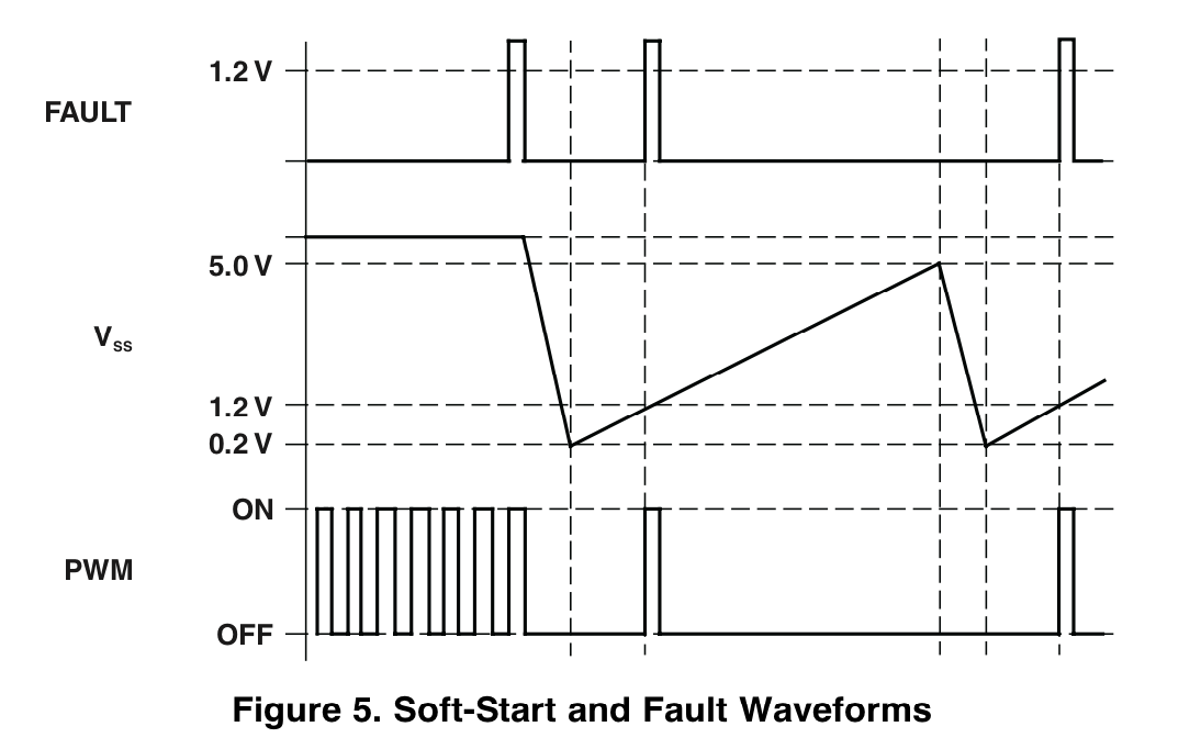
UVLO, Soft Start, and Fault Management
Soft start is programmed by a capacitor on the SS pin. At power up, SS is discharged. When SS is low, the error amplifier output is also forced low. While the internal 9-μA source charges the SS pin, the error amplifier output follows until closed loop regulation takes over.
Anytime ILIM exceeds 1.2 V, the fault latch is set and the output pins are driven low. The soft-start capacitor is then discharged by a 250-μA current sink. No more output pulses are allowed until the soft-start capacitor is fully discharged and ILIM is below 1.2 V. At this time, the fault latch resets and the chip executes a soft start.
Should the fault latch get set during soft start, the outputs are immediately terminated, but the soft-start capacitor does not discharge until it has been fully charged first. This results in a controlled hiccup interval for continuous fault conditions.
 
It looks to me that the 5v is dead. I don't find it on Q234, or IC206, or IC205, or IC202. At Q203 I find 4.5v at the base and 0 on the other two terminals. ZD checks as a diode, but is not limiting the voltage. The base of Q234 is 0 without an input on the white wire and 0.7 when there is. The other two terminals are always 0.
 
i use a really tiny sharply pointed tip on my meter leads in order to puncture thru the plastic clear coating on the board, which seems especially thick down in the LV section. A sharp dental pick tool can also be used to cut the coating and tweezers used to remove it from around solder joints.

We verified that the 5V power supply for Vcc was working earlier with the measurement of voltage on pin 7; the 5V regulator is on the bottom layer, IC 209, pin 6. It uses the "15V" supply of TP201 to create the 5V and then passes traces of an internal layer to various via pads. It's possible that the traces have been vaporized by an overvoltage event, but usually there would be some sort of visual indication.
 
Here is the block diagram of the UC2825 chip functions:
HAWu7b4.png


And a diagram of how the SoftStart (pin 8) and Current Limit (pin 9) work to turn the chip OFF and ON:
zC9tK4r.png
 
And here is a sketch of the DCSW circuit for now:
HymhZNf.png


If any of the OR gate inputs are Hi, [e.g. pin 10 or pin 12], then the output will be Hi, and that will drive the gate of Q203 to pull the SoftStart pin 8 Low, which will shutdown the PWM controller.

Some of my earlier logic and comments may have been incorrect about the purpose of DCSW--it appears to be a switch which can Start or ShutDown the converter depending upon if it is High or Low.
 
i hope this is a break thru in understanding some of the logic.

The two [dual comparator]op amp outputs of IC102 "277" on the HV Section sketch operate as a Logical OR to drive the photocoupler PC101 if either conditions are reached. i believe this is used to measure for either an UnderVoltage or OverVoltage condition of the HV input. Either condition drives the photocoupler which causes a change of state for it's output, which is connected to an inverting buffer gate of IC205 pin 1, which outputs into pin 10 of the OR gate IC206 [ shown in the DCSW sketch above]. The output of this gate then controls the SoftStart pin 8 of the PWM Controller IC201.

So if the HV is not within the range determined by the 3rd resistor chain feeding the [Comparators]Op Amps, then gate 10 will be set Hi and the PWM controller will not be able to do it's SoftStart.

So your HV of ~225V is enough to start the TR105 and get the secondaries up, but doesn't meet the necessary conditions of the IC102 [Comparator] OpAmp, and the PWM is being commanded not to Start.
 
I finally discovered that this discussion was continued on the next page this morning. So I charged up the 120v batteries to full charge and now have 240v. I still have 0v on pin 8 of IC201. Checking on IC206 pin 12 is high. Where is that from?
 
Pin 12 is related to the Temperature Sensor signal on TP217. It is a thermistor and mine measured 127KΩ at room temperature. Pin 12 is also related to another gated signal which i haven't gotten to the end yet to know, but would guess it might be the output current sensor (just a guess based upon the location of the logic gates).

It you read thru my last few posts, i don't think 240VDC is high enough to pass the OpAmp section of IC102 to start. This would be seen by pin 10 of IC206 being Hi.
 
That's not what i meant--i measured the sensor itself, disconnected from the board. There are too many other resistors involved to measure resistance at the TP. You would measure a voltage at TP217 when the unit is powered up.

So measure the thermistor resistance by itself first, then plug it into the board and measure the TP voltage when it has power.

Please provide more complete data when you try to test, start it, make a reading, etc. for example what is the total HV you are trying to use, do you have a 12V aux connected to the output, etc. i won't know if you don't tell me and some of this could affect other circuits.

i haven't calculated the [Comparator]op amp voltage limits, but i suspect that above 360 and below 270, the PWM will not start. The Pin 10 voltage should go Low when it is happy. We don't want the photocoupler to switch, that will raise the voltage on pin 10.

What about the voltage on pin 12 of IC206? Actually the voltage on pins 8 thru 13 of IC206 would give an idea of what is preventing the start.

The switching will not start until pins 8-13 of IC206 go Low. So [a Hi or about 5 volt] on the white wire of CN201, and if all the conditions are happy, all should go Low. Then the pin 8 on IC201 can rise up to 5V and start the PWM switching.
 
1.3k across the thermistor. 4.74v at TP217. Pin 12 of IC206 is 4.94v.

One leg of the photocoupler is 0v, and the other leg is also with 240v. With 303v the other leg goes to almost 5v.
 
Back
Top