Gen1 DCDC Converter Troubleshooting and Repair

Mitsubishi i-MiEV Forum

Help Support Mitsubishi i-MiEV Forum:

This site may earn a commission from merchant affiliate links, including eBay, Amazon, and others.

kiev

Moderator
Staff member
Joined
May 3, 2015
Messages
2,624
Location
The Heart o' Dixie
The DCDC converter is a separate board in the bottom plenum of the OBC and needs a separate thread for troubleshooting and repair.

Index in post #1
Pictures in post #2
Schematics in post #3
Components and Datasheets post #4
Faults and Trouble #5->
 
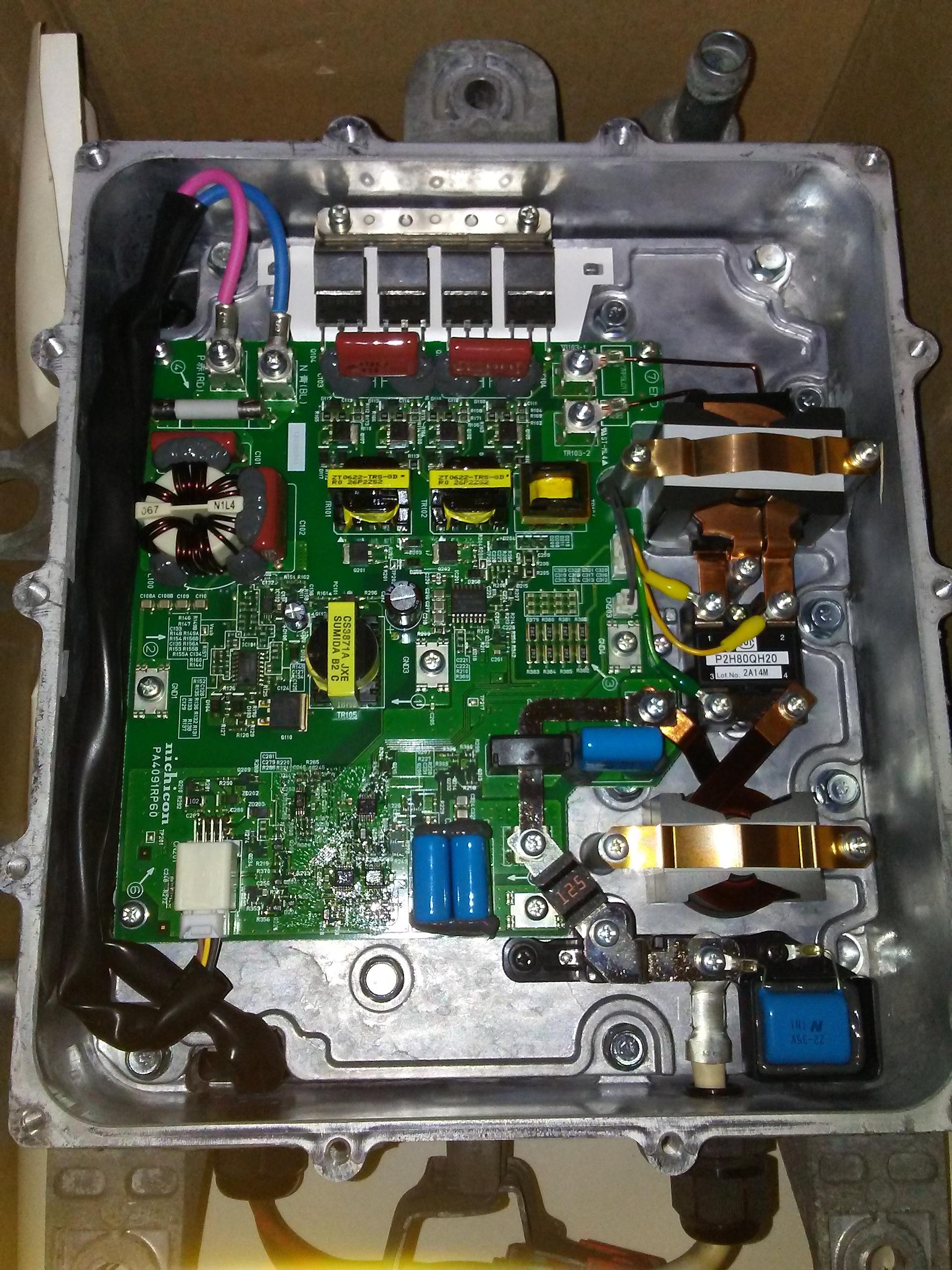
Pictures here,

bottom cover of OBC removed, the DCDC is in this lower plenum, only 5 wires to CN201, 450V 20A input fuse, 125V output fuse,
v3HHWSy.jpg


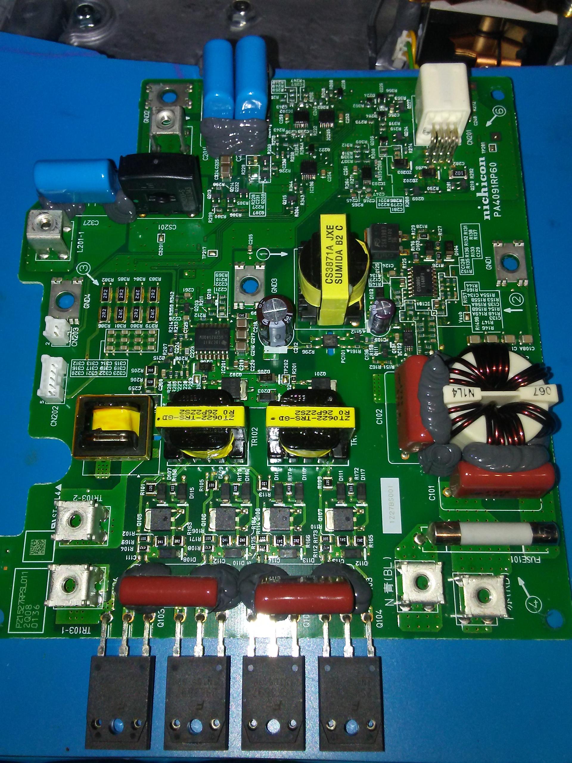
DCDC board removed, MOSFETs are clamped to heatsink for cooling,
dB4O8hQ.jpg


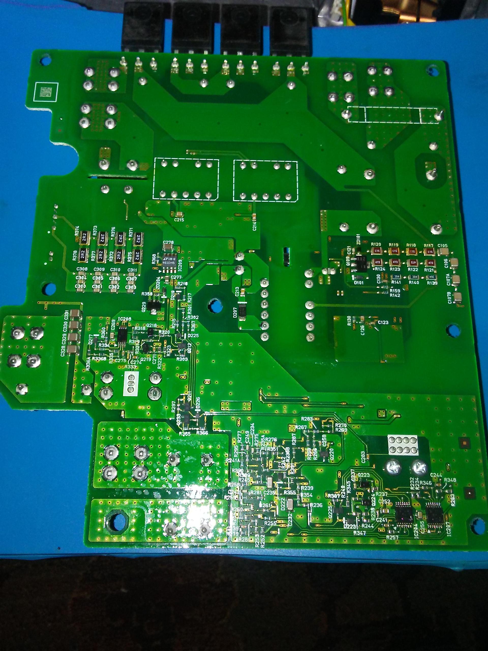
bottom side of the DCDC board, no microcontroller found,
CrU7HsI.jpg


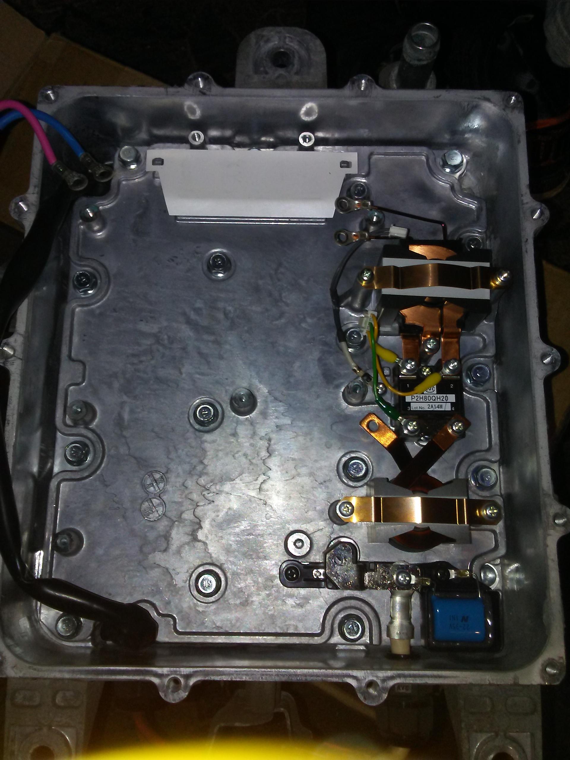
Heat-sinked components attached to cold plate, MOSFETs, Transformer, Diode Module, Output Inductor,
OHVRkrN.jpg
 
Schematics here,

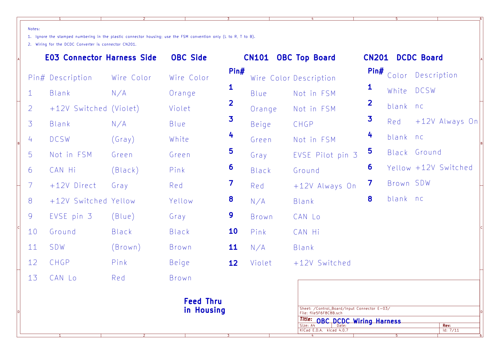
The E-03 connector to the OBC and DCDC converter
j8KrMsT.png


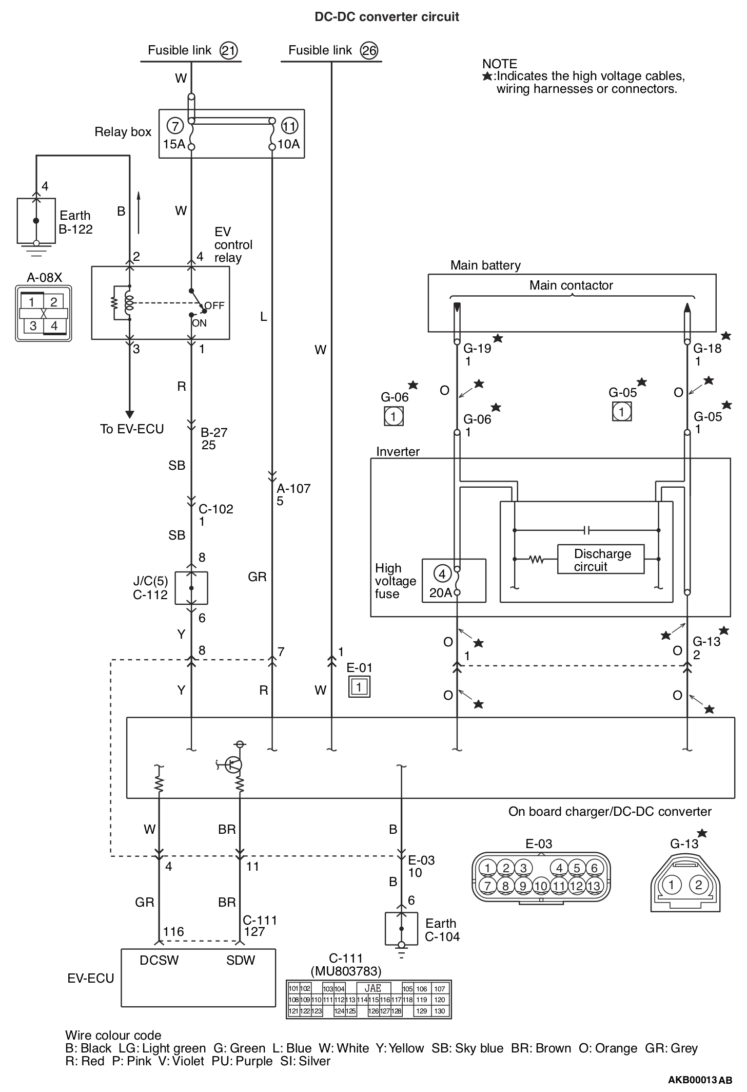
FSM wiring diagram
YxCBhtF.png


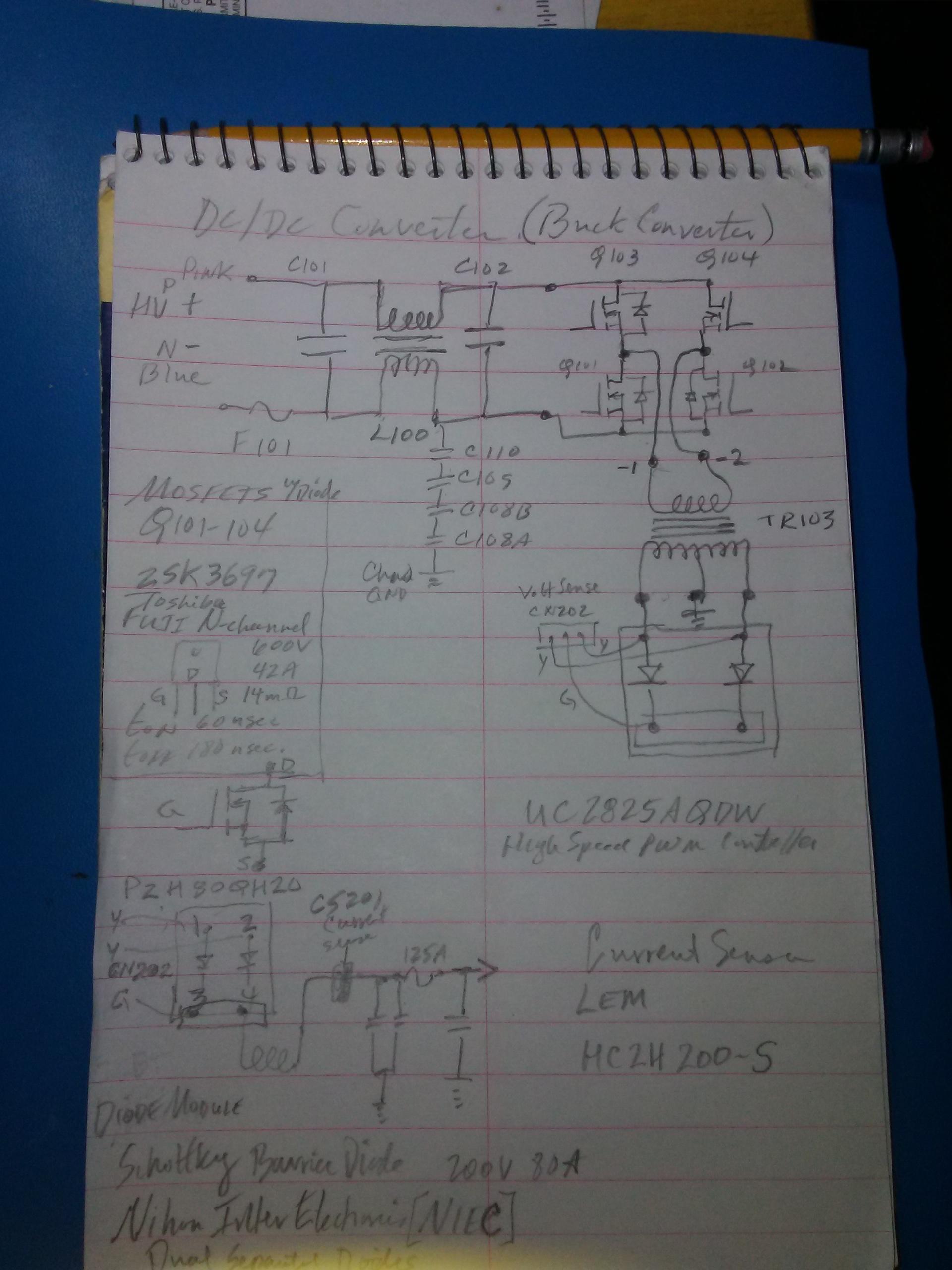
Sketch of high power component trace of the Buck Converter
zPNlYnE.jpg


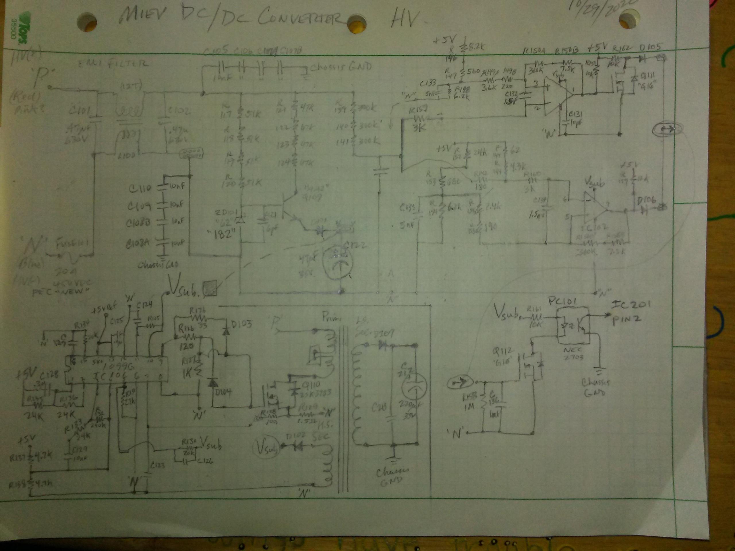
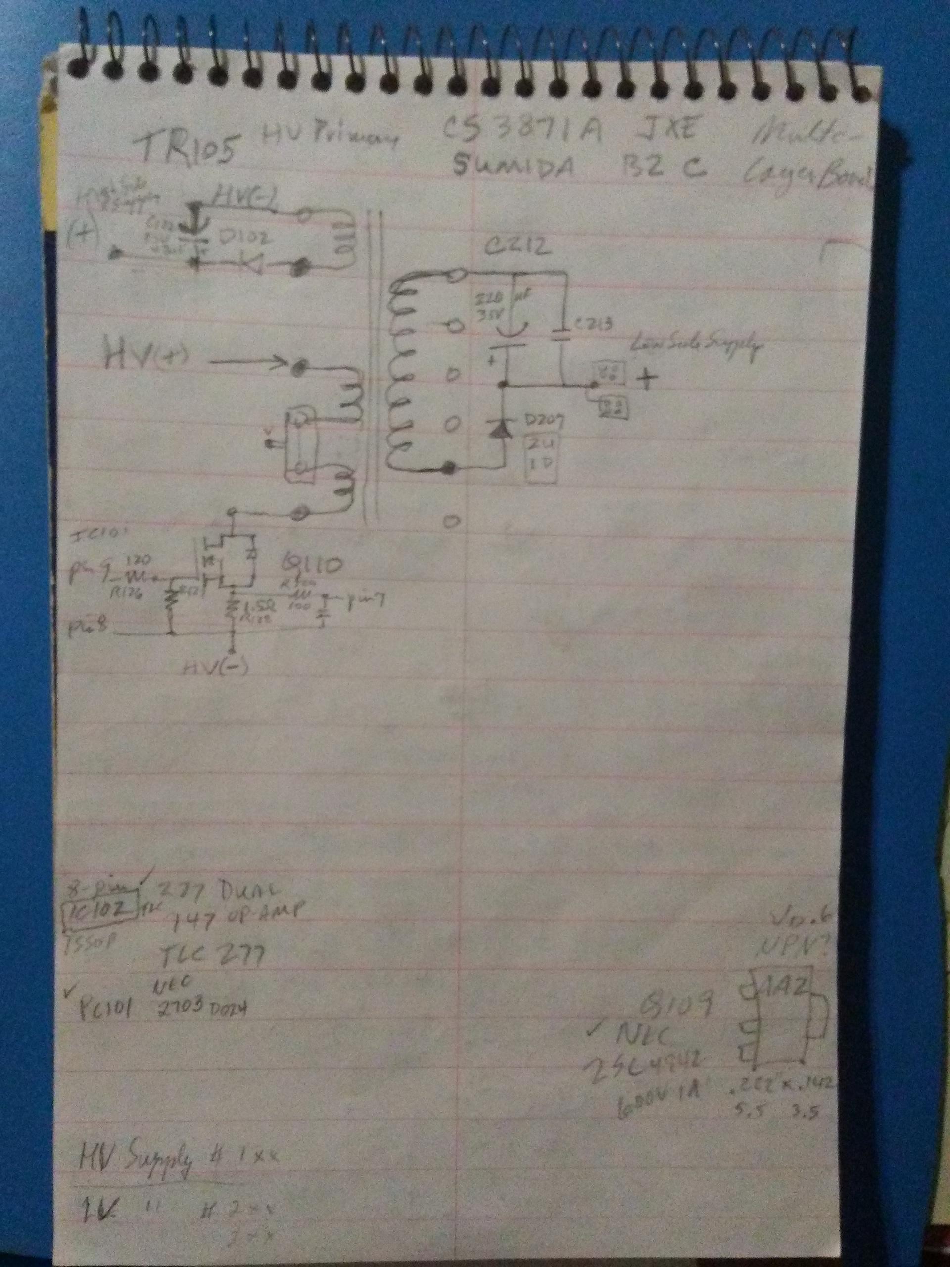
Sketch of HV Input section that creates secondary supplies for startup [IC101 and IC102]
ZBmd8ac.jpg


Sketch of the "DCSW", the white wire on pin 1 of CN201 [appears to be a Start or ShutDown Switch]
HymhZNf.png


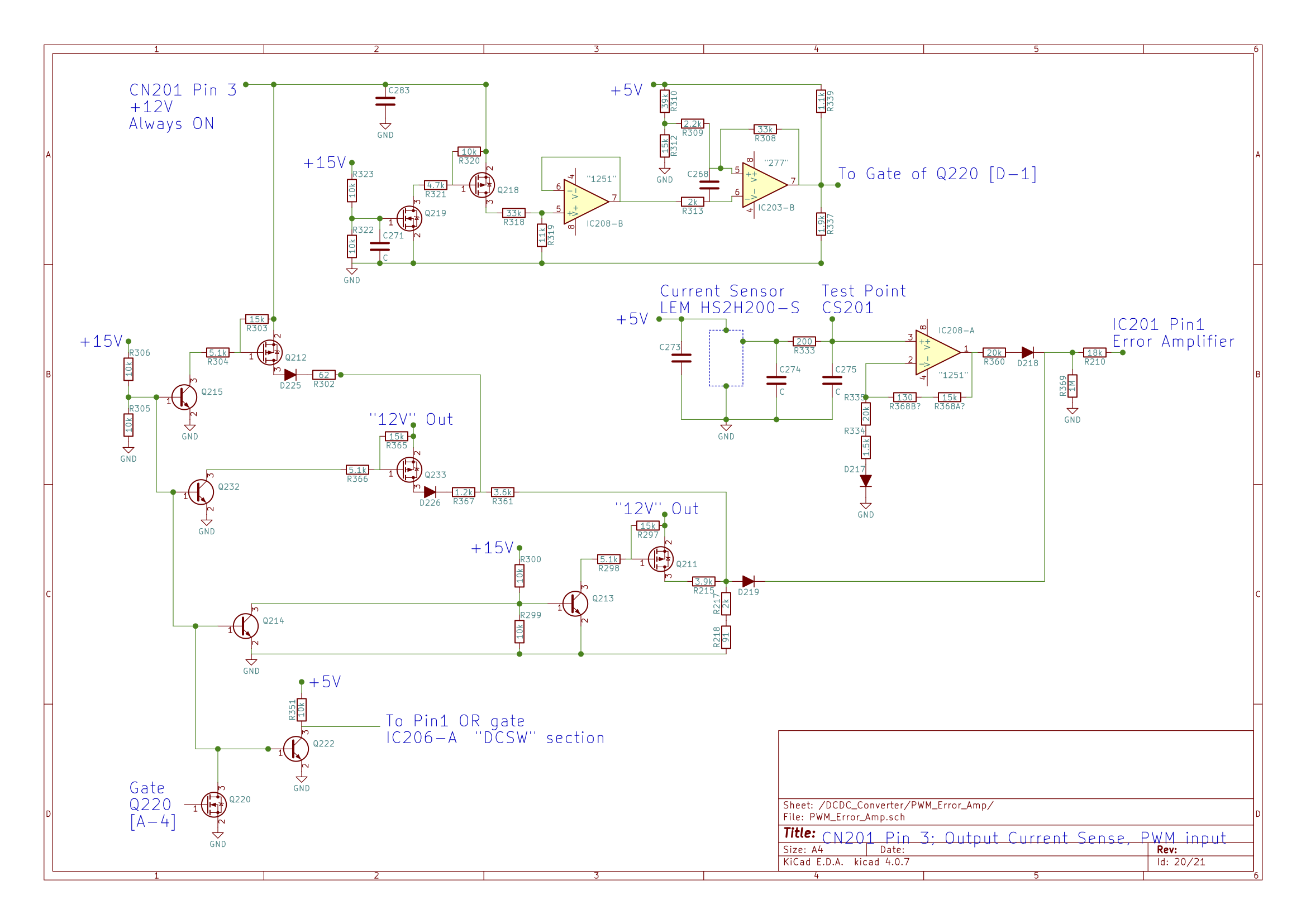
Pin 3, 12V Always ON; Current Sensor; PWM Error Amplifier input
1YqyE5o.png


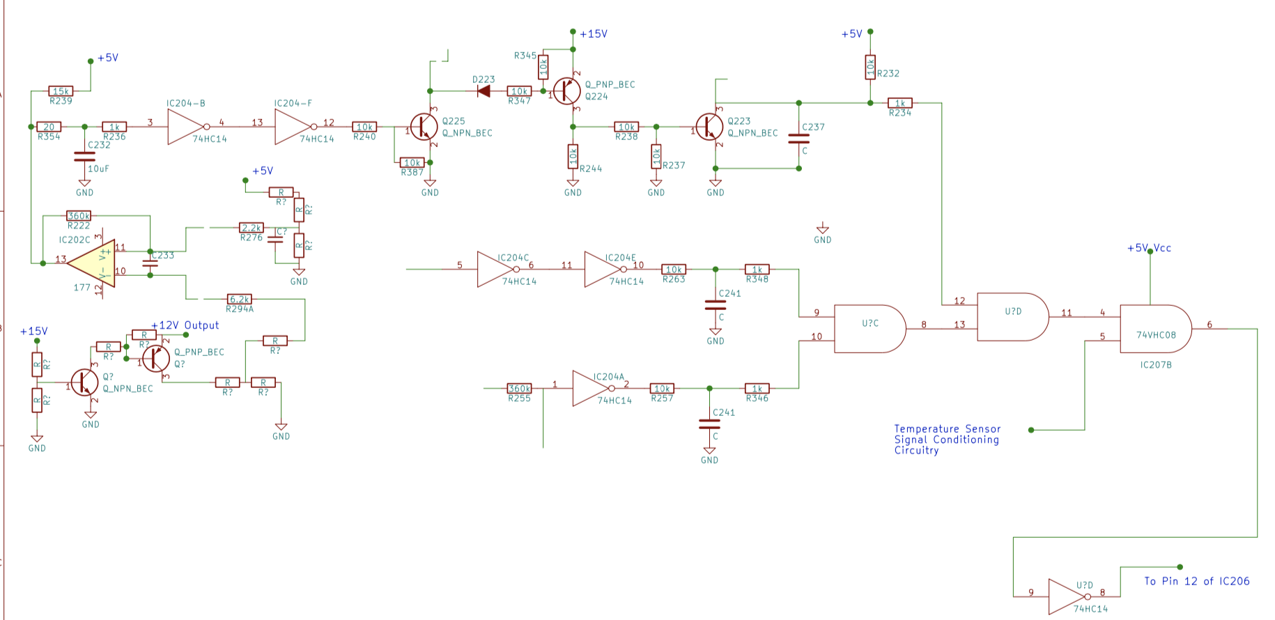
Soft Start command of IC201 PWM chip related to presence of voltages (+12 pin3, output 12, +15 TP201) and output current [signal for AND gate of IC207-D pin 12] and temperature signal.
wcslaLN.png


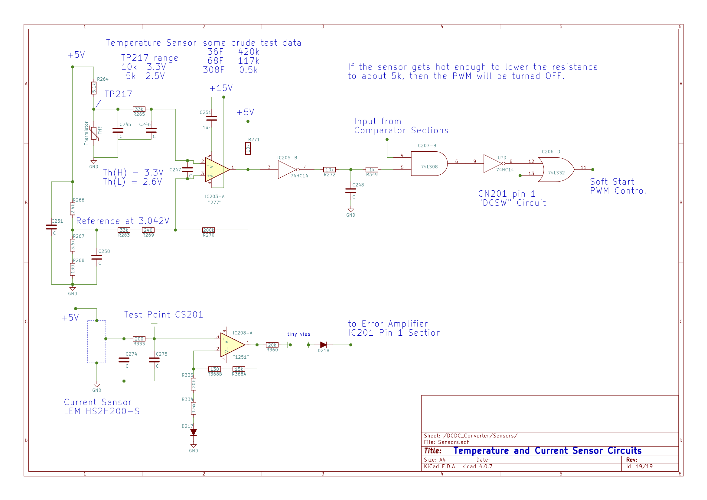
Temperature and Current Sensor Conditioning and contribution to the control of the PWM chip
ZaDdxw1.png


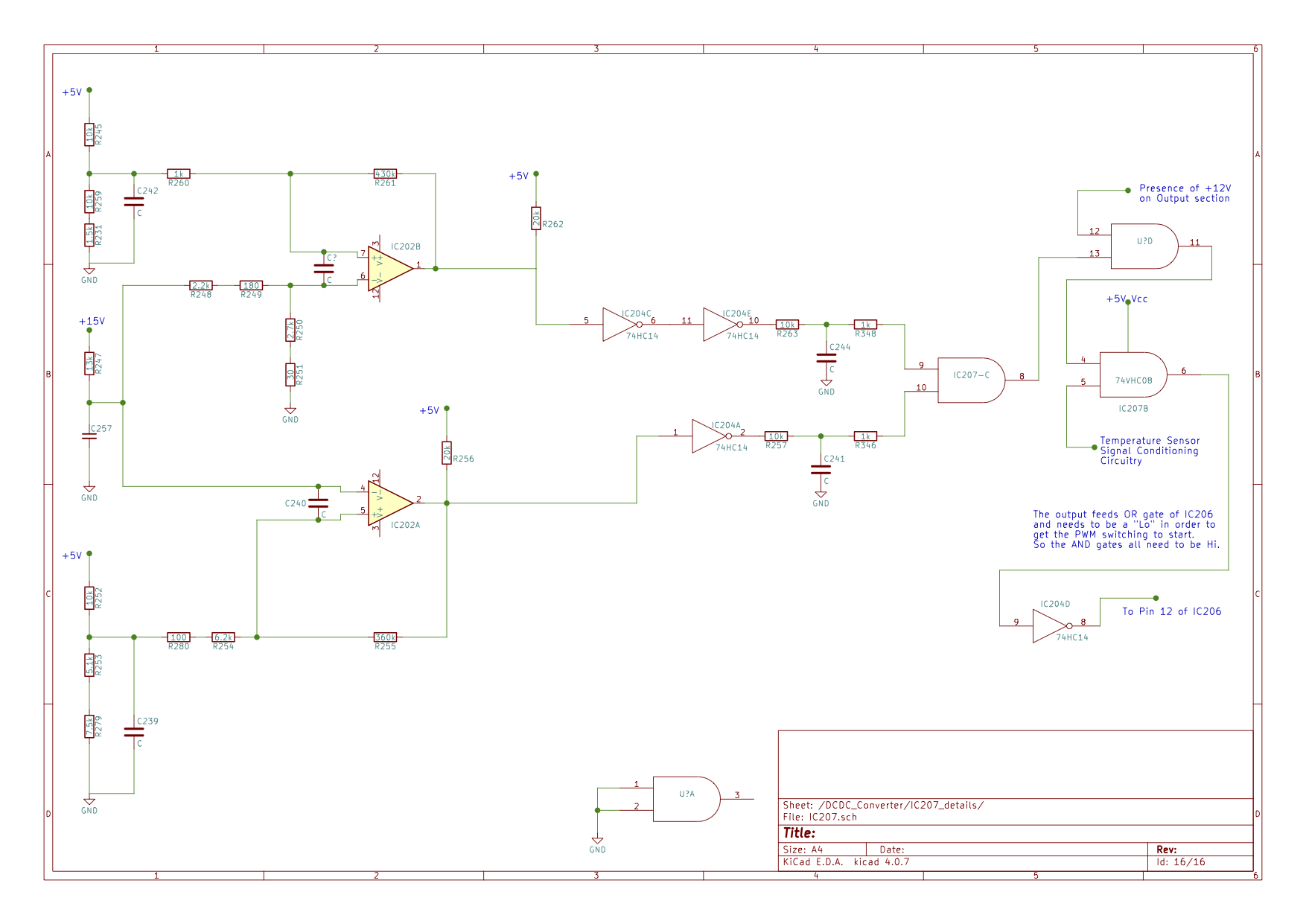
Soft Start command leg for the TP201 voltage, the "15V" secondary supply created by the TR105, using the IC202 -A and -B Comparators with hysteresis switching band to filter nuisance oscillations.
IBeg39R.png


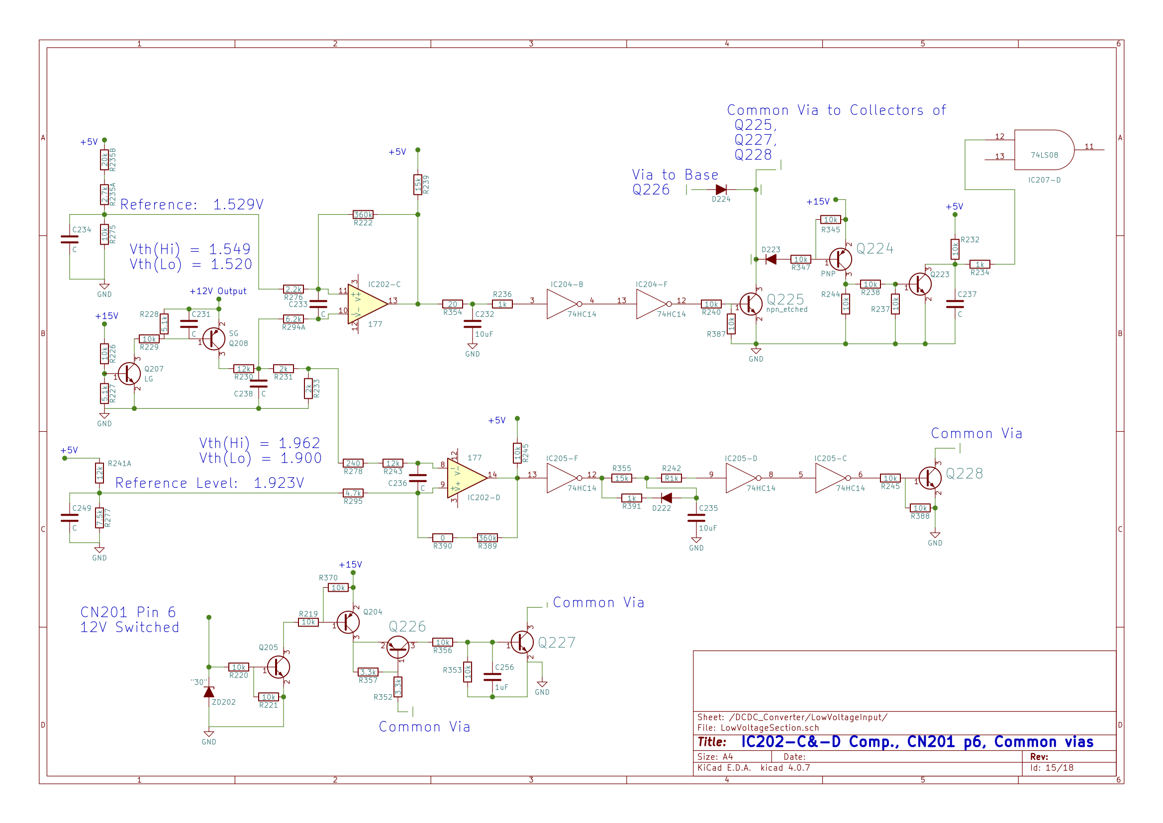
The IC202 Comparator -C and -D redrawn for easier analysis of the threshold and signal paths (Output 12V) used to feed the AND gate of IC207-D pin 12
[edit]
plus found a cluster of Common Vias linking CN201 pin 6, the Switched 12V input.
piJqyfM.png
 
Components and datasheets here,

The HV components have reference designators in the 100-series; the LV side components are -200 and -300 series. e.g. resistors, capacitors, transistors, ICs.

FUSE101, 450V 20A, marked "NEW"

IC209, Linear Tech LT1461DH5, LDO 5V reference, https://static6.arrow.com/aropdfconversion/b3fcd775414358d81f9c4170fe3a25b851538c67/1461f.pdf

Q229, marking code "CGRZ", 2SC5053, NPN 50V, 1A,

IC101, NEC uPC1099G, switching regulator, https://www.datasheetarchive.com/pdf/download.php?id=d0ee29cce8e9c9dd89fa4a4c02a63a692ac8e4&type=O&term=UPC1099

IC102, etched ?, likely an NEC uPC277 dual comparator;
https://www.renesas.com/us/en/doc/DocumentServer/006/G17934EJ3V0DS00.pdf

IC208, NEC uPC1251 dual op amp, https://datasheetspdf.com/pdf-file/1037858/Renesas/UPC1251/1

IC202, NEC uPC177GR, quad comparator, https://pdf1.alldatasheet.com/datasheet-pdf/view/216924/NEC/UPC177GR-9LG.html

IC203, "277" NEC uPC277, dual comparator, https://www.renesas.com/us/en/doc/DocumentServer/006/G17934EJ3V0DS00.pdf

PC101, NEC PS2703 photocoupler, https://media.digikey.com/pdf/Data%20Sheets/NEC%20PDFs/PS2703-1.pdf

Q110, Fuji 2SK3983 N-MOSfet, 900V, 2.6A, 6.4Ω, https://americas.fujielectric.com/files/2SK3983-01L.PDF

Q109, NEC 2SC4942, NPN 600V, 1A, https://alltransistors.com/pdfdatasheet_nec/2sc4942.pdf

Q101-104 are Fuji 2SK3697 N-MOSFETs, 600V, 42A, 14mΩ, https://americas.fujielectric.com/files/2SK3697-01.PDF

Diode Module, Nihon Inter Electronics, P2H80QH20, https://www.digchip.com/datasheets/download_datasheet.php?id=1620301&part-number=P2H80QH20

Small signal transistors identified by marking code and reference designators:
"K N", PMV48XP or Toshiba 2SJ305 P-channel FET; Q211, 212, 218, 233

"L 6", NEC 2SC1623 NPN; Q205, 207, 213, 214, 222, 223, 227, 232, 234

"S 6", seems to be PNP ; Q208, 210

"G16", seems N-mosfet; maybe IRL2502. Q203, Q111, Q219, Q220; https://alltransistors.com/pdfview.php?doc=irlml2502pbf-1.pdf&dire=_international_rectifier


IC201, TI UC2825AQDW, High Speed PWM Controller (FET gate driver), https://www.ti.com/lit/ds/symlink/uc2825a-q1.pdf

IC204, IC205; VHC14, Hex Schmitt Inverter, https://media.digikey.com/pdf/Data%20Sheets/Toshiba%20PDFs/TC74VHC14F,%20FK,%20FN,%20FT%20Rev2006.pdf

IC207, VHC08, Quad 2-In AND gates, https://www.onsemi.com/pub/Collateral/MC74VHC08-D.PDF

CS201, LEM HC2H200-S, Hall-Effect Automotive Current Transducer, https://www.lem.com/sites/default/files/products_datasheets/hc2h200-s%20clips.pdf

Transformers:
TR101, TR102, ZT0622-TRS-GD, Gate Drivers for Q101-104

TR103, Step-down Power transformer mounted to heatsink, TDK 202V0A3

TR104, ZC19A105, signal transformer for output of power transformer

TR105, CS3871A JXE SUMIDA, HV primary with 2 LV secondaries

Inductors:
L201, large flat-wire output inductor, TDK 202V0A1
 
I see that I was numbering the connector terminals from the drawing, but should have been using a mirror image. With the functions in your table, the voltage checks make sense.
It seems that the DCSW and SDW are the CAN Buss communication and likely the output control lies on the board, not from the EV-ECU. So it looks like the control chip should run when powered up without HV to the FETs.
My ohmmeter checks haven't indicated anything unusual.

Elden
 
i started a separate thread for DCDC troubleshooting with pictures, schematics and datasheets. Can you do a diode check on the Mosfets, Q101-104? Also Q110.
 
All five look OK to my vom.
Should we continue this on the other thread?

Elden

ModEdit: Previous discussion moved into this thread for completeness 27 Oct. 2020
 
Sure let's move it over to there.

@JoeS, or some other moderator; Please move this page 63 over to the Gen1 DCDC Troubleshooting thread. Thanks
ModEdit: Previous discussion moved into this thread for completeness 27 Oct. 2020
 
I find many components on the board that are not in your description of it's function. Some are no doubt involved with the CAN functions, but it appears there are important connections between the 12v PWM control generation and the HV transistors. There are five labeled transformers and L100 is labeled as an inductor, but seems to be two in magnetically coupled inductors.

Since the static test haven't revealed the problem, I'm inclined to attempt to power up the 12v section and see what seems to be happening. With only a VOM, I'm uncertain whether I will be able to identify the failure.

Elden
 
I connected 12v between gnd(10) and 12v(7) and 12v switched(8). It produced nothing that I could find. I couldn't find any supply voltage on any pin of IC201 or IC101 or IC102. I assume there are voltage regulators involved. Maybe the failure is in that portion of the circuit. I did find that the gnd planes of the OV section and HV sections are not connected. The HV gnd is connected to the HV fuse 101.

Elden
 
This would make more sense with a schematic, but here is a summary of some findings. i used the same convention for terminal numbering of CN201 as is used up in CN101, i.e. pin 1 is in the bottom right corner and pin 8 in the top left corner looking into the PCB connector.

So CN201 Pin 1 is the white wire, which is the "DCSW" from the EV-ECU found in the FSM. i traced this to the Soft Start pin 8 of the PWM controller chip IC201. i'm guessing this discrete provides the start command for the DCDC.

Pin 3 is the red wire, +12V Hot all the time. This is routed to the emitter of Q212 on the bottom layer of the board. More work is needed to ring it out.

Pin 5 is the black wire, chassis ground.

Pin 6 is the yellow wire, +12V switched by ignition. This line is clamped by a zener marked "30" ZD202 to ground, then it passes to the emitter of Q210 marked "S6". The collector goes to a 1k resistor R292 and then on to Pin 7, which is the brown wire and signal "SDW" of the FSM. The base of Q210 is pulled low thru the collector of Q209 "L6", the base of Q209 is controlled by the OR result of pins 1and 2 to IC206. There is a multitude of op amps, OR, AND logic, plus op amps, but i couldn't get thru it all.

Pin 7: The EV-ECU can sense the status of the DCDC with this signal, if it goes Hi to 12V then the DCDC is working okay; if not then something is faulty and it's time to shut down.

There is no microcontroller and no CAN buss. It is all analog circuits on a multi-layer circuit board (the +5V and chassis ground appear to be carried on internal planes).

Power Supplies:
The TR105 is a stepdown where the HV is pulsed thru the primary and two LV supplies are created in the secondaries. One secondary is used for the supplies on the HV side of the isolation gap in the PCB, e.g. for IC101 which controls the switching of Q110 to pulse the primary. The other secondary is used on the LV side of the gap and provides several supply functions: 1. Vcc supply for certain ICs directly, e.g IC202 comparator;
2. provides a voltage for the TR101,102 gate driver isolation transformers (also pulsed primaries with switching controlled by IC201); 3. It provides a feed to IC209 for creation of a reference +5V for Vcc of most all of the op amps and logic chips.

DCSW maybe means DCDC Converter Start/Shutdown Wire
SDW maybe means Sense Wire?
 
So it looks like very little will work on this board without power to the HV side. So what starts the switching in the HV circuit so TR105 has an output?

Elden
 
sketch from tracing notes, haven't had time to draw it up in Kicad. Not shown there is that the (-) side of C212 gets connected to chassis ground. The HV side of TR105 is referenced to the pack HV(-). There is about 1/2" wide isolation gap in the planes of the pcb between the HV and LV stuff.

ucToB9k.jpg
 
If I understand this, there are two buck converters. The major one controlled by IC201 providing 12v for the battery, and a smaller one controlled by IC101 providing power for most of the electronics including IC201. IC201 is started by the EV-ECU and controls Q101-Q104. IC101 starts by the connection of the HV to the system which provides enough energy through TR105 to boot strap that converter. The 12v supplies to the dc-dc converter do little more than monitoring.

Assuming the Aux battery charging converter was working extraordinarily hard because my Aux battery was failing, what seems likely to have failed when the snubber capacitor failed and blew the MCU fuse?
 
eldenh said:
If I understand this, there are two buck converters. The major one controlled by IC201 providing 12v for the battery, and a smaller one controlled by IC101 providing power for most of the electronics including IC201.
My initial reaction was nah, surely they would just run IC201 from +12 V. But of course, +12 V might be +8 V some of the time, and it's the job of the DC-DC to charge the auxiliary battery no matter how flat it might be (though there may be some limits).

So yes, you'll need some HV to test this. But maybe 30 V from a current limited power supply might be enough to get things tested. Though more likely it will need a bit more. As Kiev will recall, Elcon/TC chargers for example would start with about 56 VDC at the mains input, so perhaps 54 V after two diode and other voltage drops. 56 V was convenient for me, as I had a dual 30 V power supply, so I could put the two halves in series. They would sometimes start on less than 56 VDC, but not always or reliably.
 
eldenh said:
I connected the HV input to 59vdc and got 59v on the gates of Q101, Q104 and Q110 but don't see that it is running.
59 V on the gates?! With respect to HV-?

What about the sources?

It seems like perhaps the fuse or other component in HV- is open circuit.

Edit: first order of the day would IMHO be Vcc to GND on the two main chips, IC101 (pin 11 wrt pin 6) and IC201 (pin 15 wrt pin 10). There must be something tricky getting power to IC101 before it can power itself, a sort of bootstrap arrangement. This might need a little help starting off 59 V instead of the usual 300+ volts.
 
It sounds like those Mosfets are shorted internally. [unless the fuse is blown like coulomb mike has identified]

looking at the overview sketch only the Drain of Q103 and Q104 should read the HV(+) value, but the Gates should have no voltage until the switching power supply starts and the PWM controller gets the Soft Start command, then the Gate voltage shouldn't ever exceed +/- 30VDC (max in specs). And certainly the lower FETs shouldn't be seeing any voltage, although the Source of Q101 and Q102 should be at HV(-). i would guess that the taps to the TR103 would probably also be reading the HV(+), e.g, the 59V of your power supply (with respect to the HV(-) terminal.

Remove the MOSFETs and check the big brown caps, C103 and C104 if they have punched thru. Then check for shorted resistors, diodes, transistors in that area between the Mosfets and the gate driver transformers.

If the FETs are shorted, then when removed it may be that the bootstrap switching of TR105 may start and you could read the secondary DC of C105 and C212.
 
Back
Top