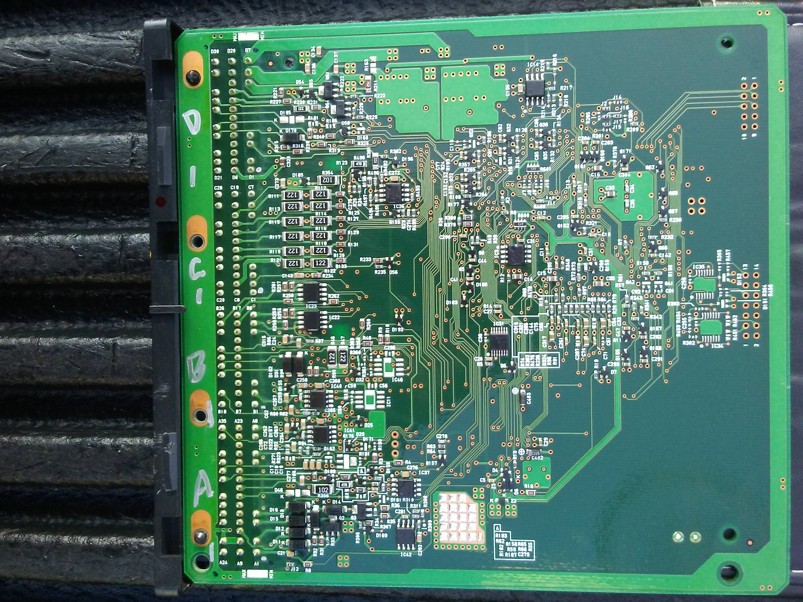
This may be overly optimistic and entirely premature, but here are pictures of the top and bottom of the board to get it started.
Con1 is the main box connector which is subdivided into 4 separate connectors marked A-D on the board.
Con2 and 3 look like unpopulated programming ports, such as JTAG for the micro and something with a bunch of pins for an eeprom.
Also some little bitty 3- and 4-pins for Con4 and Con5, likely for some sort of program or testing power supplies.
IC1 has mitsubishi logo and is marked MH8106F 115A105 U0.
IC2 has a big mits logo and is marked E350B SC111528BAF M66E 263 QDE1124D.
Anybody interested feel free to jump in and bite off a slice--ain't gonna be easy but a whole lotta fun...
Top side
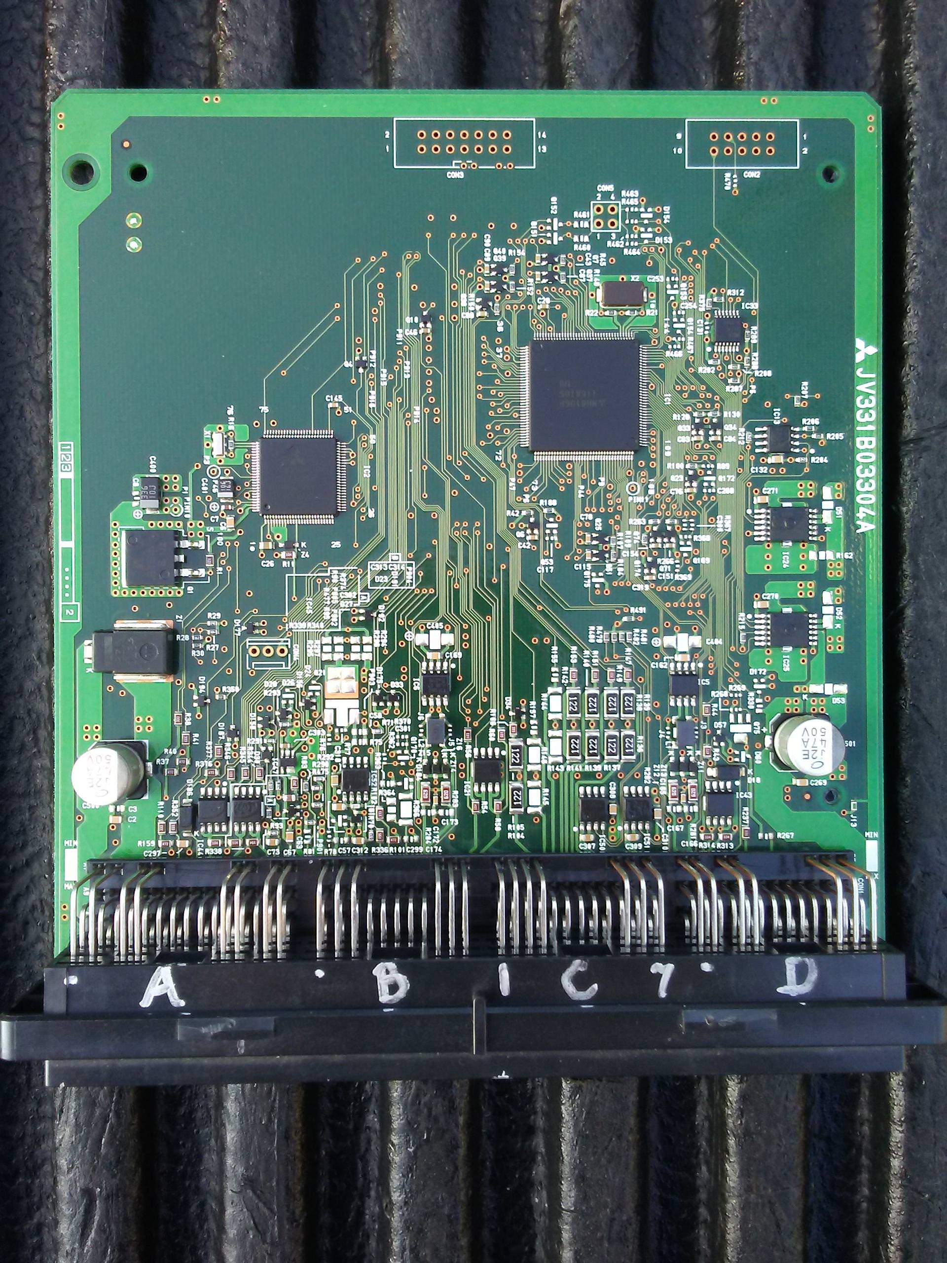
Bottom

Con1 is the main box connector which is subdivided into 4 separate connectors marked A-D on the board.
Con2 and 3 look like unpopulated programming ports, such as JTAG for the micro and something with a bunch of pins for an eeprom.
Also some little bitty 3- and 4-pins for Con4 and Con5, likely for some sort of program or testing power supplies.
IC1 has mitsubishi logo and is marked MH8106F 115A105 U0.
IC2 has a big mits logo and is marked E350B SC111528BAF M66E 263 QDE1124D.
Anybody interested feel free to jump in and bite off a slice--ain't gonna be easy but a whole lotta fun...
Top side

Bottom
