CMU Board : notes, eprom, cell re-numbering, CAN messages

Mitsubishi i-MiEV Forum

Help Support Mitsubishi i-MiEV Forum:

This site may earn a commission from merchant affiliate links, including eBay, Amazon, and others.
i don't remember why, but the Seiko data sheet for the S93C76A seemed to be a good match, http://www.farnell.com/datasheets/46815.pdf
and there seems to be an ABLIC version that is about the same also.

i had plenty of false readings using the Github arduino code which may have been related to the use of the ORG pin on some of the other versions such as the 93C76C, but i don't recall that either.
 
DBMandrake said:
Finding the secret sauce to easily renumber CMU's using a readily available third party diagnostic tool such as Hobdrive / icarsoft etc (no soldering/eeprom swapping) would be a breakthrough for the DIY and aftermarket repair and servicing of these battery packs.
I'm making slow progress on reading CMU firmware, and I think I've got to the stage where I can speculate how this happens.

1) It may be necessary to start with a CAn bus message (on the bus that CMUs are on, I don't know if messages from the main CAN bus pass through the BMU to the CMU) with message ID 0x3C3 (the same one that does bypassing), with D4 set to 4 (or at least, has D4[2] set). You can't say "leave the bypass bits alone", so you have to choose what you want with the bypass bits if you want to send a 3C3 message. All zeroes for the rest of the packet should force no bypassing.

2) The BMU sends the following 5-byte packet over the daisy chain, which connects to UARTD1 on the CMU processors:
00 FF 0F 00 0E
The first byte (D1) appears to be unused, and it initialised to 0. But the BMU may send different contents.
The next 3 bytes are what sets the CMU ID. We want CMU ID 1 at the start of the chain, and strangely this is in about the middle of a table. So we need 6 non-zero pairs of bits, starting with the LSBs of D2, indicating that we don't want IDs 7, 8, ... 12. With bits 4 and 5 set to zero, the first CMU sets its ID to 1, and the rest of the bits of D2 and D3 have to be zero, or it will get cancelled. I have set both bits in the pair in my example; sometimes the CMUs send only odd bits (so e.g. D2 would be 0x55), or even bits (0xAA), or both bits (0xFF, as I have here).
The last byte (D5) is the sum of bytes D2-D4.
[ Edit: these packets are probably sent at 300bps; see next post. ]

I believe that a task function is awoken that will save the new ID into EEPROM (the first word, it seems to me, though it's possible that it moves around).

So: not terribly convenient perhaps, but it should be possible to make up a gizmo that plugs into the appropriate connector and sends the bytes.

[ Edit: "first byte" -> "first word", "first BMU" → "first CMU"]
 
Anyone know what the crystal frequency is? The processor manual (if I have the right one) says it will work with 4.0 - 20.0 MHz crystals.

I don't know how to look this one up:

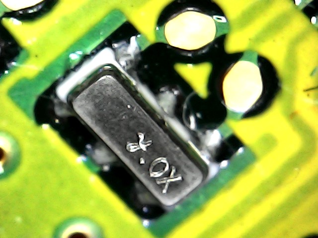
O8l7r1G.jpg


It's almost like y.0X, with the leading "y" in a cursive font. [ Edit: either dot zero X or dot oh X. ] Maybe the cursive "y" is a manufacturer's logo. I did a quick search, but I don't know how to find those either.

It looks like the bit rate of uart1, which does the auto renumbering, is the clock frequency divided by 130*8 = 1040, so it might be 9.98 Mhz for 9600 bps. I'd say 10.000 MHz (9615 bps, 0.1% fast) would be close enough. Perhaps the "X" represents the roman numeral 10.

[ Edit: Oops, that's Uart 0, which seems to be for testing only (the TXD0 and RXD0 pins seem to come out only to testing pads). Uart1 seems to have /256 and /130, for 1·10⁶ / 256 / 130 = 300.48 bps. ]

Or it could be 20.000 MHz and 19 200 bps. [ Edit: 20 MHz and 600 Hz. ] But I would think that they'd want to stay away from the absolute upper frequency limit of operation. Especially on a CMU, where power consumption is paramount. [ Edit: also, 9600 and 300 bps seem "more standard" to me than 19 200 and 600 bps. ]
 
On my board the crystal is marked "X0 . n" . It appears to be a murata part, 10Mhz, based upon the marking code,

https://www.murata.com/products/productdata/8801161904158/SPEC-CSTNE10M0G550000R0.pdf?1559743212000
 
kiev said:
It appears to be a murata part, 10Mhz, based upon the marking code
Brilliant, thanks! [ Edit: I wasn't expecting a "resonator"; I don't really know the difference. I remember Murata made 455 kHz ceramic resonators (for radio IF filters) in the 1970s. ]

So that's confirmed then: the auto-renumber data is at 300 bps, and the test/debug data is at 9600 bps.
 
coulomb said:
...
1) It may be necessary to start with a CAN bus message (on the bus that CMUs are on, I don't know if messages from the main CAN bus pass through the BMU to the CMU) with message ID 0x3C3 (the same one that does bypassing), with D4 set to 4 (or at least, has D4[2] set). You can't say "leave the bypass bits alone", so you have to choose what you want with the bypass bits if you want to send a 3C3 message. All zeroes for the rest of the packet should force no bypassing.

2) The BMU sends the following 5-byte packet over the daisy chain, which connects to UARTD1 on the CMU processors:
00 FF 0F 00 0E
The first byte (D1) appears to be unused, and it initialised to 0. But the BMU may send different contents.
The next 3 bytes are what sets the CMU ID. We want CMU ID 1 at the start of the chain, and strangely this is in about the middle of a table. So we need 6 non-zero pairs of bits, starting with the LSBs of D2, indicating that we don't want IDs 7, 8, ... 12. With bits 4 and 5 set to zero, the first BMU sets its ID to 1, and the rest of the bits of D2 and D3 have to be zero, or it will get cancelled. I have set both bits in the pair in my example; sometimes the CMUs send only odd bits (so e.g. D2 would be 0x55), or even bits (0xAA), or both bits (0xFF, as I have here).
The last byte (D5) is the sum of bytes D2-D4.
[ Edit: these packets are probably sent at 300bps; see next post. ]
...

There is a fellow interested to command bypassing/balancing in his pack our of the car, so i want to revisit your post here to understand the process. i get easily crossed up with the byte and bit conventions.

In 1) above, is only D4[2] necessary to be set with everything else zero, i.e. no target voltage in D1 D2 ?

So a CAN message such as 0x3C3 [8] 00 00 00 04 00 00 00 00 sends the CMUs an alert that "i want to do bypass balancing and the details will follow", or
sending 0x3C3 [8] with D1-D8 all zeroed says "i don't want to do any balancing"?

The 0x3C3 PID is only found on the CMU CAN buss, it is not sent over the main CAN buss. This is true for all the BMU PIDs such as 0x6n1 thru 6n4, the voltage and temperature data, these are only on the CMU CAN. These get reformatted in the BMU and sent out as PIDs 0x6E1 thru 6E4 on the main CAN.

Regarding 2) above,
"With bits 4 and 5 set to zero, the first BMU sets its ID to 1" means the first CMU?
and
the bits 4 and 5 are which byte D2[5-4] or D3[5-4] ?

Is D4 ever used or always zero?

For your example if i display the D2-D4 bytes as bit pairs:
D1 00
D2 FF= 11 11 11 11
D3 0F= 00 00 11 11
D4 00= 00 00 00 00
D5 0E

Do these 12 bits represent the 12 CMU (as 6 bit pairs)?

What 5 bytes would the BMU need to send to the daisy chain (the first CMU) to cause them to auto number?

What would the last CMU send back to the BMU, is there a confirmation of success/completion?
 
kiev said:
There is a fellow interested to command bypassing/balancing in his pack our of the car, so i want to revisit your post here to understand the process.
Wonderful!

I get easily crossed up with the byte and bit conventions.
So do I. I call the first CAN bus data byte D1, I suspect that the convention is to call it D0. I can't seem to find the answer to that anywhere; it's frustrating.

In 1) above, is only D4[2] necessary to be set with everything else zero, i.e. no target voltage in D1 D2 ?
I believe that the answer is yes, effectively. Every 0x3C3 packet seems to set the threshold voltage, so leaving the first two bytes zero means "set the threshold voltage to 2.1 V" (there is a 2.1 V offset). But leaving later bits zero means "don't bypass", and any subsequent 0x3C3 packet will over-ride the threshold voltage, so as far as I can see, there will be no harm in leaving the first two bytes zero.

So a CAN message such as 0x3C3 [8] 00 00 00 04 00 00 00 00 sends the CMUs an alert that "i want to do bypass balancing and the details will follow", or
sending 0x3C3 [8] with D1-D8 all zeroed says "i don't want to do any balancing"?
I believe it's saying "I want to initiate CMU renumbering, and set the bypass threshold to 2.1 V, and the bypass function to be performed is "no function". It's not quite "do nothing", because if it was bypassing earlier, this will cancel that bypassing. But we probably don't want to be bypassing while we change ID numbers around.

The 0x3C3 PID is only found on the CMU CAN buss, it is not sent over the main CAN buss. This is true for all the BMU PIDs such as 0x6n1 thru 6n4, the voltage and temperature data, these are only on the CMU CAN. These get reformatted in the BMU and sent out as PIDs 0x6E1 thru 6E4 on the main CAN.
I suspected as much. So this means to initiate renumbering, assuming that I'm correct in needing this special 0x3C3 packet, we'd have to set up some small computer to spit out this packet just on the CMU bus. Hopefully, this won't be too hard if the battery box is opened up, as it would obviously have to be in order to replace a CMU board.

I note that the conversation now switches from CAN packet 0x3C3 to the 5-byte serial data packet on UARTD1 of the CMUs. This had me confused for a while.
Regarding 2) above,
"With bits 4 and 5 set to zero, the first BMU sets its ID to 1" means the first CMU?
Yes, sorry. I had a propensity to call the CMUs BMUs back then. I think I'm better now :shock:

and
the bits 4 and 5 are which byte D2[5-4] or D3[5-4] ?
D3, by which I mean the third byte,

Is D4 ever used or always zero?
Yes, it's used if referring to CMUs 3-6 (see below).

For your example if i display the D2-D4 bytes as bit pairs:
D1 00
D2 FF= 11 11 11 11
D3 0F= 00 00 11 11
D4 00= 00 00 00 00
D5 0E

Do these 12 bits represent the 12 CMU (as 6 bit pairs)?
Yes. I can't find that table right now, but it seems to work like something like this: [ edit: this is wrong, see next post ]
Code:
D2 FF=  11 11 11 11
CMU id  12 11 10  9
D3 0F=  00 00 11 11
CMU id   2  1  8  7
D4 00=  00 00 00 00
CMU id   6  5  4  3
Why they screw up the ordering, I have no idea. Fortunately, as long as I got it right (gulp), the details don't matter, as we just have to send the right data to what will become CMU1, and the CMUs should figure out what data to send to renumber the others sequentially. But that means we need our special renumbering gadget to also send this special 5-byte packet at 300 bps to UartD1 of CMU1.

What 5 bytes would the BMU need to send to the daisy chain (the first CMU) to cause them to auto number?
I believe that the example I sent (00 FF 0F 00 0E at 300 bps) is what the BMU would send, if it received the renumber command from a MUT, and is what we should be sending too.

What would the last CMU send back to the BMU, is there a confirmation of success/completion?
Good question, and one that whoever tries this out will be keen to know. I'll try and answer that soon. It's taking me a while to get my head back into this space.
 
coulomb said:
Yes. I can't find that table right now, but it seems to work like something like this:
Code:
D2 FF=  11 11 11 11
CMU id  12 11 10  9
D3 0F=  00 00 11 11
CMU id   2  1  8  7
D4 00=  00 00 00 00
CMU id   6  5  4  3
I found the table; I call it CmuIdMaskTbl . It's actually like this:
Code:
D2 FF=  11 11 11 11
CMU id  10  9  8  7
D3 0F=  00 00 11 11
CMU id   2  1 12 11
D4 00=  00 00 00 00
CMU id   6  5  4  3

I suppose that this might be useful if trying to renumber a single CMU on the bench, not in a live battery. So to set a CMU to ID 9, the bit pairs would be 00 11 11 11  00 00 00 00   00 00 00 00 or 3F 00 00 for the middle 3 bytes. Or for ID 6: 11 11 11 11   11 11 11 11   11 11 11 00 or FF FF FC. Basically, send pairs of 1 bits until the ID you want, with the IDs numbered 7 8 9 10 11 12 1 2 3 4 5 6, then send pairs of 0 bits to the end, starting at the LSB of the first byte (which is the second byte of the whole packet, after the unused zero byte).

Edit: Except that maybe the bit pairs should be 01 or 10, instead of 11; I still haven't figured out what that's about.
 
kiev said:
What would the last CMU send back to the BMU, is there a confirmation of success/completion?
I can't see a CAN packet at the end of the process.

But I think you can tell from the last bit pair what happened:
11 if the last bit pair was 11 (unexpected, nothing happened)
01 if the last bit pair was zero, but that didn't result in a change of ID
10 if the last bit pair was zero, and that did result in a change of ID

So if you are setting the whole string of 12 CMUs at once, then if bits 2 and 3 of the middle byte transmitted out of CMU12 was 10, then some ID did change along the way. So generally that last packet would be 00 FF F8 FF F6 on success, if I didn't screw up. And there are plenty of ways I could well have screwed up.

If anyone is good with assembly language and wants to check my work, here is a link to my CMU firmware IDA Pro listing (.LST) file. PM me if you want the Ida Pro database file (.IDB). I warn you that even for assembly language, this one is pretty weird, so this will be a hard slog. 544 kiB zip file, containing a 6 MB listing (plain text) file.

https://drive.google.com/file/d/1yQpAqB57Yc0RZtexVNW7XRBpqIaRYDrV/view?usp=sharing
 
Hi coulomb,

Thanks for publishing all your progress thus far! Building on your work, I've managed to figure out the renumbering process for the similar Outlander CMUs: https://openinverter.org/forum/viewtopic.php?t=2789

Many details are exactly the same as you described them. I reckon there's some chance the serial packets are the same.
 
I'm trying to repair a "red" CMU, i.e. one of the pre-2012 types with the red conformal coating.

This one is weird. There is no 5 volts on the battery side of the isolation chips. It's an 8-cell board, and I only have one 4-cell board for comparison. I traced the problem to a 2SD1584 Dpak NPN transistor. The collector is connected to the D- cell terminal, which makes no sense. I find that the 4-cell board connects instead to the A+ cell terminal!! Far more sensible, and it actually works. So the mystery is why does the 8-cell board connect to the opposite end of the set of 4 cells.

It's a multi-layer board, and I'm finding it hard to find where traces go when they connect by internal layers. I finally found that A+ after the fuse connects to a part marked H19, which appears to be a P-channel FET. Strangely, the gate to source resistor is 10k for the 8-cell boards, and 24k for the 8-cell boards. At least this part of the circuit is the same on red versus green boards; the 5  V power supply is completely different.

Has anyone had any success tracing the red board schematic, at least the part that generates 5 V for the isolation chips?

Or the P channel MOSFET circuit, on either the red or green boards?
 
coulomb said:
Strangely, the gate to source resistor is 10k for the 8-cell boards, and 24k for the 8-cell boards.
It could make some sense if there was a resistive divider, and the 8-cell boards worked on 8 cells worth of voltage. But this part of the red board circuit seems to be working on only 4 cells worth of voltage.

Just in case, I plugged in an extender board (the board for cells E-H). It's a "green" extender board, but I don't think it would make any difference; the only parts on the extender boards seem to be 4 fuses. I cranked the A+ to H- voltage up to 31 V (the highest my power supply will go), and it still drew less than 1 mA. When the isolator chips are running, the boards draw over 10 mA from 13 V.
 
Quite a puzzle for sure.

Are you saying that there is a different resistor [10k or 24k] used depending upon whether it is a 4- or 8-cell module board? Or was the different resistor related to the board color and applied to 8-cell modules?

And on the 4-cell boards, the P-FET power is taken from Cell A+ with respect to D-, but on the 8-cell boards they take that power from E+ with respect to H- ? i would guess that would be done to always reference the "Ground" level to the lowest voltage level of a module.

i've never had a red board in my hands to provide any tracing help. The green board that i used to trace was from a module that Martin bought to get replacement cells for his pack.
 
Hello everyone,
I would like to add a detail that will be useful to those who one day decide to use the battery of their Miev for another use.
CMUs boards listen, from startup, for 0x3C3 frames only if these frames are sent regularly. If the transmission of these frames stops for a moment before resuming, the balancing requests are never considered again, until the next restart of the CMUs cards.
I spent a lot of time figuring out why my battery balancing wasn't starting, so it might as well help as many people as possible.
Good day to all.
 
If the transmission of these frames [0x3C3] stops for a moment before resuming, the balancing requests are never considered again, until the next restart of the CMUs cards.
Thank you for sharing this important finding from your research--it will be very helpful. And it explains some of the strange balancing behaviour reported by others.
 
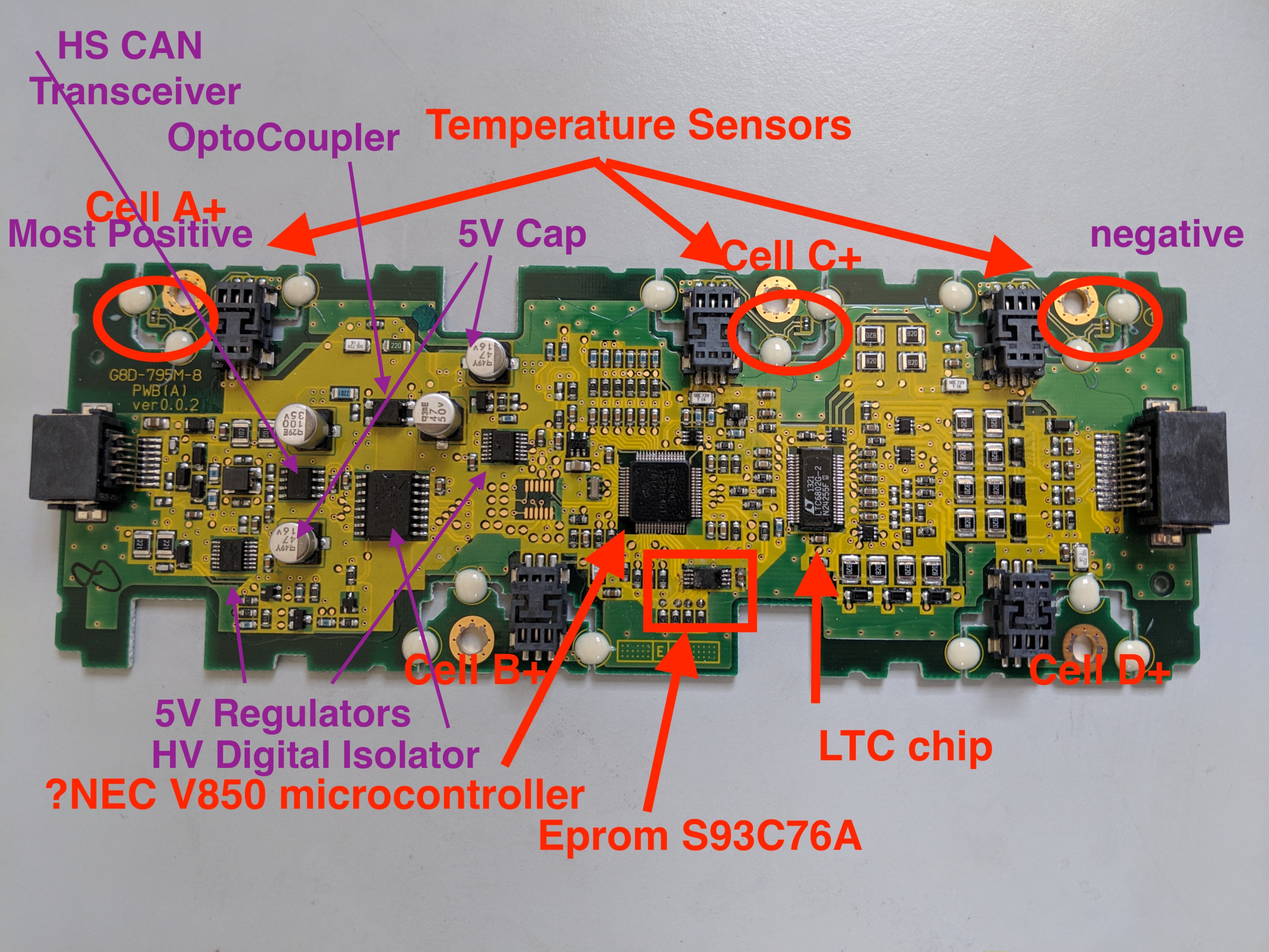
Does anyone know the part number or the specifications of the the thermistor chips? If not, does anyone have CMU boards for sale? CMU 5 H?
If I remember correctly it is the V850 that ‘reads’ the temperature sensors, while the LTC chip converts the cell voltages. Don’t think you can actually replace the sensors under the white blob.

It’s quite simple to re-program a CMU if you can’t find a CMU5..
 
They are not located under the white blob, just near it (can be seen in the picture).

i measured 3 of them on one of my boards, all reading 7.19k Ohms at 70 F, and dropping to 6.5k when heated with my finger. Physical size is 0402 inch or (1005 metric).

Based upon this i think the part number is:
TH05-3N682F for a 1% device.

Here is a datasheet for Mits chip thermistors, NTC type.
digikey datasheet
 
Last edited:
Back
Top