You are using an out of date browser. It may not display this or other websites correctly.
You should upgrade or use an alternative browser.
You should upgrade or use an alternative browser.
[ The P1A15 Troubleshooting Thread ] No READY. P1A15 error. Condenser charge timeout.
- Thread starter Lic
- Start date


Help Support Mitsubishi i-MiEV Forum:
This site may earn a commission from merchant affiliate
links, including eBay, Amazon, and others.
boothegermanshepherd
Well-known member
That sounds like a very good idea, because the only principle with my understanding is to see a specified voltage out at pin 3 after terminal 50 pulse (cranking signal), in a certain timescale.
Is the problem that the hybrid board as its alone gets too hot and doesn't dissipate the heat, unlike the main board is screwed to 5kg of alloy!
But it seems that if all other diagnosis is exhausted then it must be in the inverter, 99.9% the hybrid board, we would be better off just either repair or replacement of that board. It does seem a very basic system the more I study it but have never made or had a board made. Has anyone else been involved in that process?
[Edit march 2024: Note in the diagram below that they have used "Auxiliary battery" when it really should read "Main HV battery" ]
In this overview block diagram of the MCU there is a Voltage Sensor. This is operational all the time during driving, not just during Startup. The software in the Control is throwing this code when it detects an abnormal High Voltage condition during Start, but it will also throw a code at anytime during READY. So it is not just a ramp involved here.
Circuits that handle 360VDC are not trivial designs, and the hybrid board is just one part of the Voltage Sensor that provides isolation between the HV and LV circuits. Repair or replace is a better solution than a re-design.
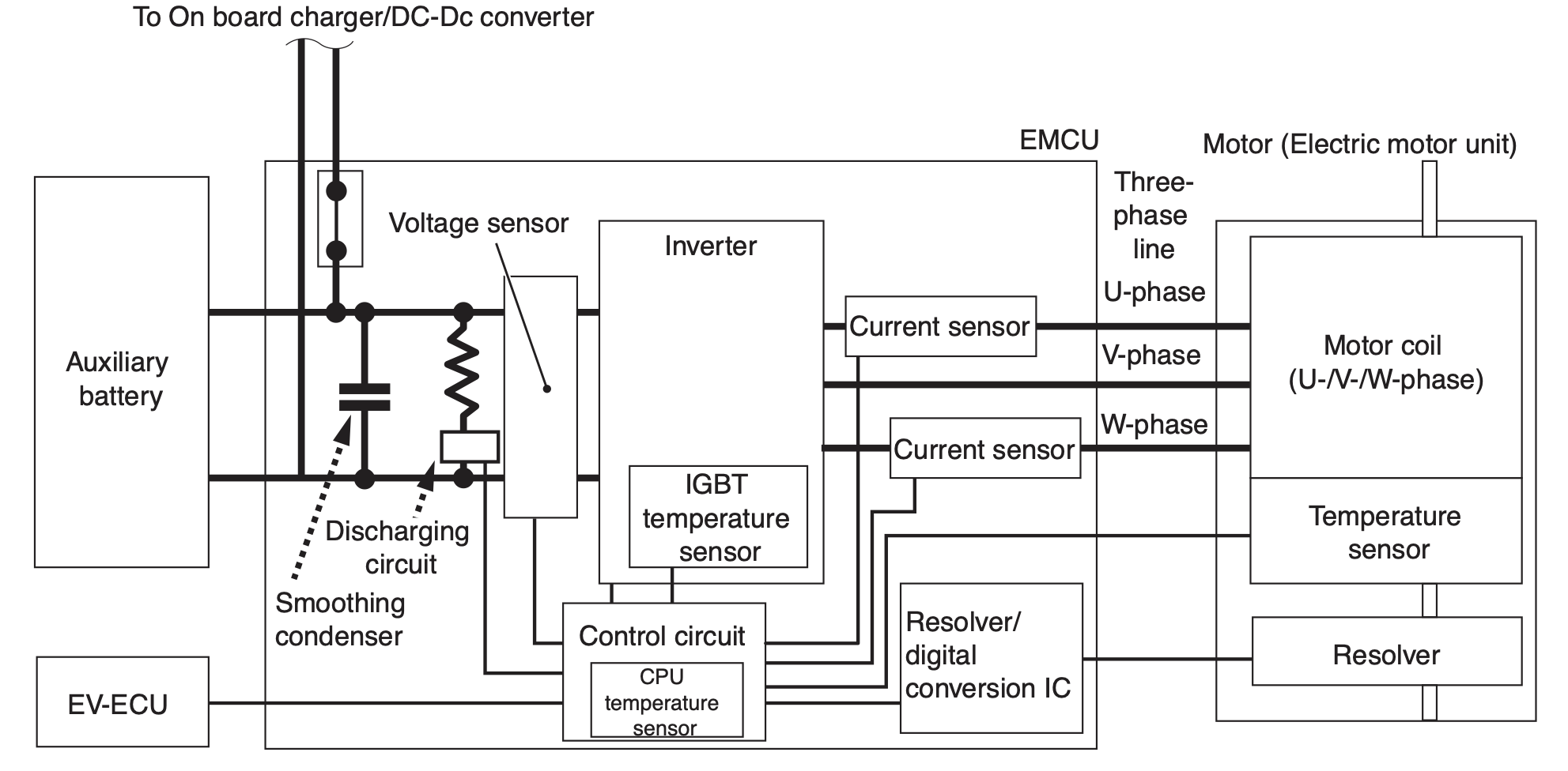
Last edited:
boothegermanshepherd
Well-known member
Thanks for the detailed explanation.
I am only feeding the hybrid board 4v on Hl and hv, is the high voltage not reduced on the wavey row of 6 resistors before hv?
I am only feeding the hybrid board 4v on Hl and hv, is the high voltage not reduced on the wavey row of 6 resistors before hv?
Regarding cooling: only the high-power transistors ( IGBTs ) in the upper chamber require cooling. They are fixed to a cold plate which is bolted to the liquid-cooled cast alloy box. There are no high-wattage components on the lower board that dissipate enough heat to require cooling. The board is screwed to stand-offs, so it is actually held some distance away from the alloy box. As a daughter-board, the hybrid probably runs marginally cooler than the main board. Bearing in mind that the lower chamber is totally sealed with no airflow and there is a fair amount of electronics on that board, it probably reaches a fairly warm but constant temperature during normal use. Personally, I think component aging is more significant in this issue.
Initially I thought that the correct hybrid board output could simply be spoofed, but now I guess that the s/ware in the EV-ECU is looking for a rising voltage sequence, not a fixed high.
[ Last year I bought a "spares or repairs" 2012 Citroen C-Zero on eBay with this specific P1A15 error. So far, due to life and Covid-19 getting in the way, I have not made any progress.]
boothegermanshepherd
Well-known member
Hi Eddie
Sounds like exactly the same one as I have just bought!
Apart from the difference of this project is getting in the way of life not the other way around!
Sounds like exactly the same one as I have just bought!
Apart from the difference of this project is getting in the way of life not the other way around!


$32.99
RAOXIO 4 Pcs Car Door Protector Edge Guards for Mitsubishi i MiEV 2009-2020, Scratch and Abrasion Resistant Car Door Edge Guards Carbon Fiber Texture Door Edge Guard Accessories
kunmingxiaojingmanshangmaoyouxiangongsi


$87.99
WYMZF Car Covers, for Mitsubishi i-MiEV 2010-2021 All Weather Outdoor Indoor Waterproof UV Resistant Dustproof Windproof Protection, Auto Accessories,B
DATONGSHIPINGCHENGQUDAYUANBAIHUODIANGERENDUZI


The more i think about it... i have to wonder why the LV supplies were not equal or at least closer in voltage--especially since they are created with respect to VL as the reference "zero". Gencis also measured unequal supplies on his board with the same 0.15 drop in the hybrid Output. So could the problem it be related to the supplies, and then something is also sensitive to temperature changes?
Also when you were applying heat to the corner (close to the TL494 PWM chip on bottom and the other 4066 on top), you were also seeing the Output drop. DId you do any localized heating around the PWM chip and the other 4066 and it's components to observe for Output shifts? And what about other components on the top and bottom--did you try it everywhere top and bottom, and only the bottom 4066 was responsible?
Not being able to clearly identify what i'm calling the 5-pin logic chip (mine is etched) is a concern because it seems to be powered by these +/- supplies, and it's output drives the B&C control lines on the bottom 4066. This seems to be a dual supply device whereas almost all the datasheets i could find with a matching pinout were only single-sided supply devices.
About the need for HV isolation:
The Input voltage signal to the hybrid should be reduced to around 4V, but what if some or all of the wavy resistor string shorts out and puts full HV pack voltage on that pin? What if the HV could get thru and onto the 12V or chassis return--then the whole car could be Hot with HV DC.
boothegermanshepherd
Well-known member
I heated components as localised as possible with a hot air gun when the hybrid was still mounted on the main board, I was unable to tell which item was causing the variation,
It was after the second test that the voltage appeared perfect with input to output, but this didn't last long
When I removed the board I tested with the tip of the soldering iron set to 200 degrees, the only item to give any variation more than 0.01v is that chip tc4066 as you say. It is a vast variation, when I cool it with pcb cleaner it rapidly changes.
I appreciate we are dealing with high voltage but my understanding also is that any high voltage leakage would cause and earth return fault and open the contactors.
coulomb
Well-known member
But single/dual supply is largely a point of view, is it not? It's presumed to be just a logic device, so it could connect to +5 and -5 V just as easily as +10 V and 0 V, as long as the inputs are somewhat close to the supply rails (whatever those rails are). No logic gate is going to take a positive rail, negative rail, and "earth". Being CMOS, the outputs will be very close to rail to rail, which is presumably ideal for the TC4066.kiev said:This seems to be a dual supply device whereas almost all the datasheets i could find with a matching pinout were only single-sided supply devices.
Even an op-amp, often thought of as a dual supply device, only actually has two power pins, positive and negative. A so-called single rail op-amp is usually designed to run with lower voltages, e.g. +5 V and 0 V, and/or can operate with inputs close to its negative supply rail. But that same "single rail" 5 V op-amp could work happily connected to +2.5 V and -2.5 V; it doesn't know the difference.
That's just the hint i needed to look at it from another view.
Toshiba made a series of single inverter logic chips with 18V Vcc, found some sheets on digikey such as TC4S584F,
https://media.digikey.com/pdf/Data%20Sheets/Toshiba%20PDFs/TC4S584F_Mar01_2014_DS.pdf
The marking code is "CA", and i found another (TC4SU69F) with "C6", and the (TC4S69F) marked "C5". i think Gencis said his chip was "C4". Mine is etched and some of the Toshiba parts are obsolete, but Rohm is a current supplier.
[edit: found a Toshiba logic gate in the SOT23-5 package marked "C4" (TC4S71F), but it is a 2-input OR gate. Pin 1 seems not to be connected to anything on the hybrid and that seems not a good design to leave an input pin floating, so maybe the "4" is an "A" ? ]
boothegermanshepherd
Well-known member
Ok so is my shopping list going to have the right items in for the recipe?!?!
Can you read any marking code on your board for the 5-pin device on the top side?
One of the higher Vcc devices from Rohm might be needed since the Toshiba may not be available.
My best guess right now for this device:
"CA" is TC4S584F, Schmitt trigger Inverter from Toshiba. digikey US, https://www.digikey.com/en/products/detail/toshiba-semiconductor-and-storage/TC4S584F-LF/870444
the equilavent Rohm part is BU4S584G2, from digikey .PL
https://www.digikey.pl/product-detail/en/rohm-semiconductor/BU4S584G2-TR/BU4S584G2CT-ND/1158709
boothegermanshepherd
Well-known member
"C5" perfectly visible
boothegermanshepherd
Well-known member
https://uk.rs-online.com/web/
The "C5" is obsolete, but the "CA" is still available from RS, stock number 144-5204,
https://uk.rs-online.com/web/c/semiconductors/logic-ics/inverters-ics/?searchTerm=Toshiba+single+inverter+gate&applied-dimensions=4294854948,4294884061,4294509563
https://uk.rs-online.com/web/c/semiconductors/logic-ics/inverters-ics/?searchTerm=Toshiba+single+inverter+gate&applied-dimensions=4294854948,4294884061,4294509563
boothegermanshepherd
Well-known member
Perfect, thank you, so how do we go about getting some boards made?
i like to use Kicad, an open source pcb design tool to draw up schematics, layout the board, generate BOM, etc. There are other free tools available out there too, it's just what you get comfortable and like to use. i have some other projects going on right now that get in the way of the fun stuff like this.
boothegermanshepherd
Well-known member
I downloaded Kicad but its way over my head!
Ill have to wait until your ready!
Ill have to wait until your ready!
boothegermanshepherd
Well-known member
Good afternoon,
Now i'm in need of some help,
Replaced TC4066 and when measuring had only 3.5v on the output, replaced it with another and now 3.775, so perhaps this is not the fault but I am aggravating it! In turn its AGGRAVATING me!
What should I replace next?
To top it off when heating the same area I have the same symptom, the output drops off!
boothegermanshepherd
Well-known member
Update
Replaced TL4066
Replaced TL4941
Replaced capacitor and resistor above +12 pin
Replaced capacitors above pin 3 return voltage
Still the same!!!!!
Any help appreciated
Replaced TL4066
Replaced TL4941
Replaced capacitor and resistor above +12 pin
Replaced capacitors above pin 3 return voltage
Still the same!!!!!
Any help appreciated
Similar threads
- Replies
- 51
- Views
- 5K
- Replies
- 1K
- Views
- 960K