You are using an out of date browser. It may not display this or other websites correctly.
You should upgrade or use an alternative browser.
You should upgrade or use an alternative browser.
Gen1 DCDC Converter Troubleshooting and Repair
- Thread starter kiev
- Start date
Help Support Mitsubishi i-MiEV Forum:
This site may earn a commission from merchant affiliate
links, including eBay, Amazon, and others.
kiev
Well-known member
[edit2] i just used a power supply to put 5V on pin 1 of CN201 and 12V on pin 6 and did not get any current flow thru the Zener diodes, so i'm thinking the "30" means 30. and not 3.0 volts. So now i'm back to thinking the discrete SDW is nominal 12V battery system voltage levels.
[edit1] i never determined the Zener voltage of ZD 202 and 203, both are marked "30", but if that means 3.0 and not 30., then what i wrote here is not correct. Maybe the DCSW and SDW are 5 or 3.3V signal levels?
[/edit]
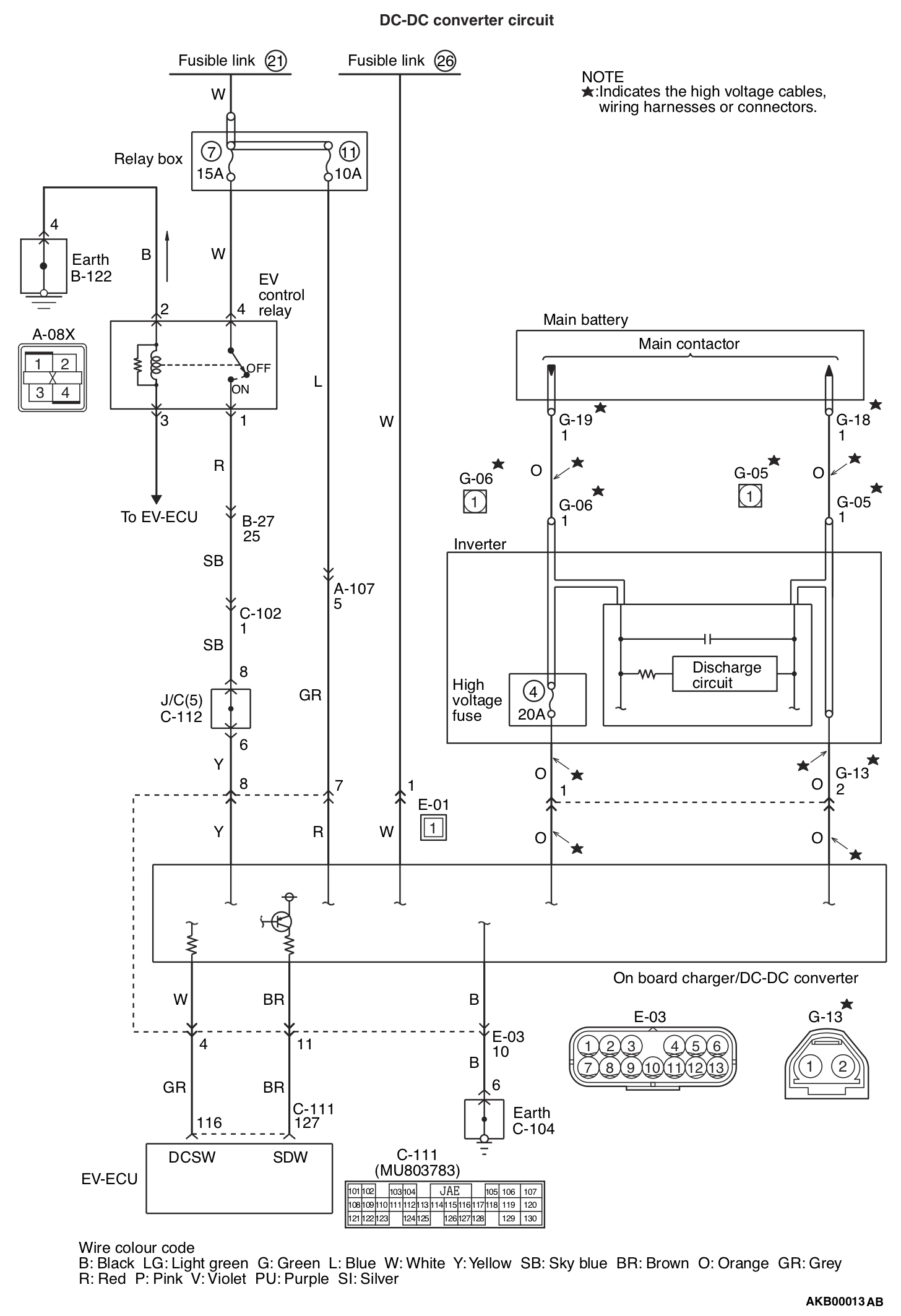
Yes you are right it is battery voltage, i.e. what i was calling the +12V Switched system voltage that comes in on the yellow wire to pin 8 of E03 connector to the OBC, and gets routed down to CN201 connector on the DCDC board pin 6.
This system voltage gets returned on pin 7 "SDW" of CN201 up to the Brown wire of pin 11 in E03 connector to the EV-ECU. This happens when the transistor Q210 is turned ON to complete the path; the drive for Q210 occurs when all the check circuits in the DCDC are "happy".
Not sure what line you are calling a 5V DCDC enable? Is the DCSW a 5V output from the EV-ECU?
This is nearly drawn out in the diagram, just draw a line from the end of pin 8 over to the top of the transistor shown on pin11 of E03.
[edit1] i never determined the Zener voltage of ZD 202 and 203, both are marked "30", but if that means 3.0 and not 30., then what i wrote here is not correct. Maybe the DCSW and SDW are 5 or 3.3V signal levels?
[/edit]
Yes you are right it is battery voltage, i.e. what i was calling the +12V Switched system voltage that comes in on the yellow wire to pin 8 of E03 connector to the OBC, and gets routed down to CN201 connector on the DCDC board pin 6.
This system voltage gets returned on pin 7 "SDW" of CN201 up to the Brown wire of pin 11 in E03 connector to the EV-ECU. This happens when the transistor Q210 is turned ON to complete the path; the drive for Q210 occurs when all the check circuits in the DCDC are "happy".
Not sure what line you are calling a 5V DCDC enable? Is the DCSW a 5V output from the EV-ECU?
This is nearly drawn out in the diagram, just draw a line from the end of pin 8 over to the top of the transistor shown on pin11 of E03.
kiev
Well-known member
i've never measured the DCSW signal at pin 116 of the EV-ECU, or at pin 4 of the OBC E03 connector. Has anyone done this?
[edit]
Looking in the FSM, pin 116 is the "DCSW" and listed as the 12V DCDC converter shutdown signal, and the measurement should show battery voltage.
http://mmc-manuals.ru/manuals/i-miev/online/Service_Manual/2012/54/html/M154920100002700ENG.HTM
Pin 127 is the "SDW" and listed as 12V DCDC converter drive signal
Electric motor switch: ON (before electric motor unit start), should read 1 V or less
Electric motor switch: ON → START position (after electric motor unit start), should read Battery voltage.
From my look at the circuit boards and wire colors, i think DCSW is an output of the EV-ECU and SDW is an output of the DCDC.
i wonder if there is a typo or error in the FSM, where DCSW should be the Enable or Drive signal, not the shutdown; and SDW is the Shut Down, not the drive?
Overview of DCDC Converter in the Technical Information Manual,
http://mmc-manuals.ru/manuals/i-miev/online/Service_Manual/2012/54/html/M254950030002900ENG.HTM
kiev
Well-known member
Thank you for the update that is very helpful information for this thread. Good luck on your repairs and getting it all working again.
Thank you to. IDK how many days I would spent trying to make this work, if not your help. And if only I always recheck any connections, it would be faster. So, I may say even more, cos of my "fails"
- No charger connected or half plugged gives battery errors.
- Brown wire to yellow, as dc-dc do gives sometimes error on dash
- Brown wire to red one I don't even tried, cos it may give some errors immediately.
- Brown wire to gnd gives absolutely nothing
- Brown to white gives no errors on dash and no errors in diagnostic software.
Looks like switched +12 and DCSW shows up in the almost same time, but DCSW turns of little earlier than switched +12. Just in case someone will need this information to use i-miev gen1 with another dc-dc or use "stock" dc-dc without i-miev
Similar threads
- Replies
- 12
- Views
- 2K
- Replies
- 0
- Views
- 11K
- Replies
- 7
- Views
- 1K