kiev
Well-known member
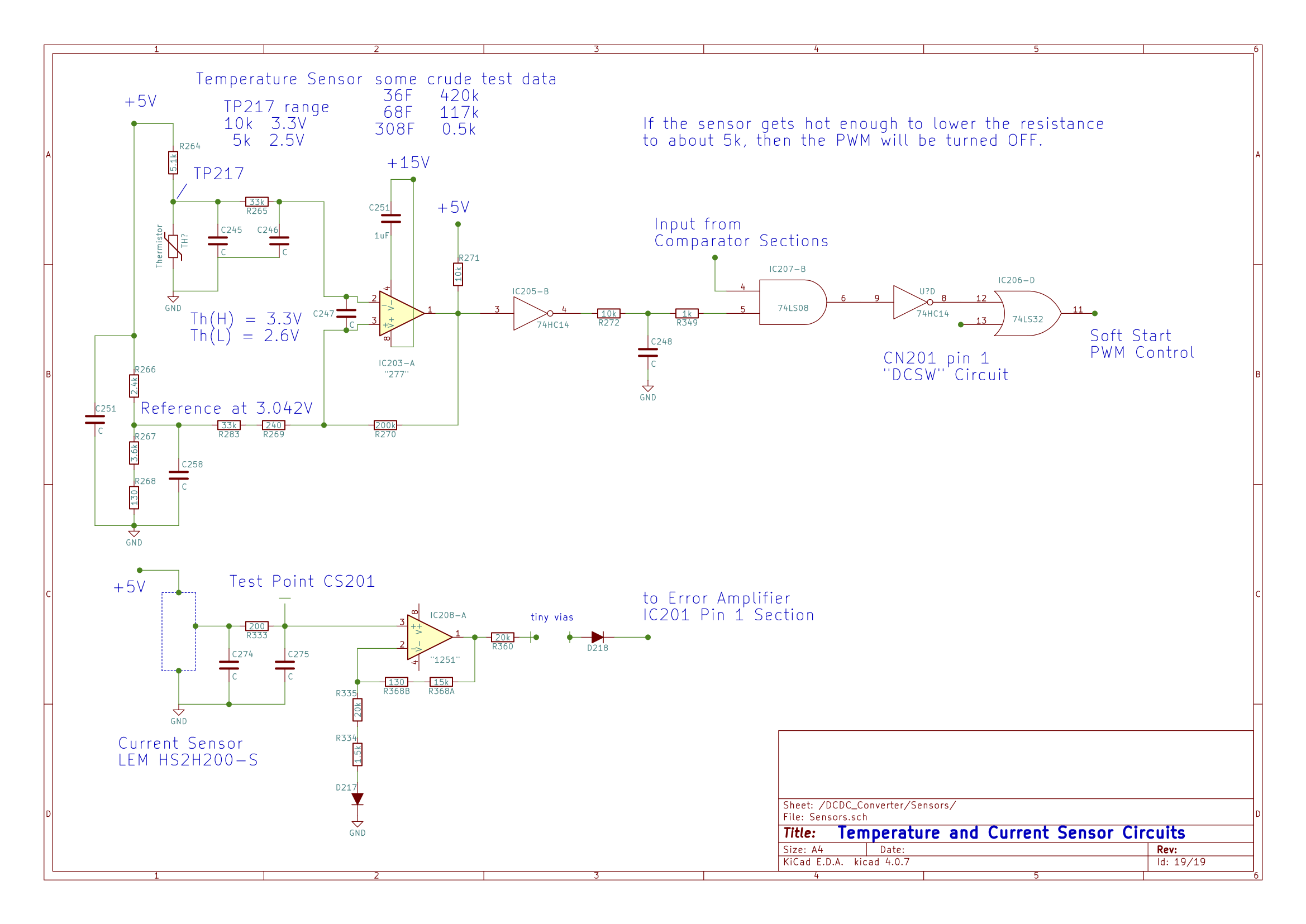
i've changed my mind on the identification of IC102 and IC203, from dual op amps to dual comparators. i see a common hysteresis design used on these circuits as on IC202 which seems to be a quad comparator. The only dual op amp seems to be IC208, etched and barely marked "1251".
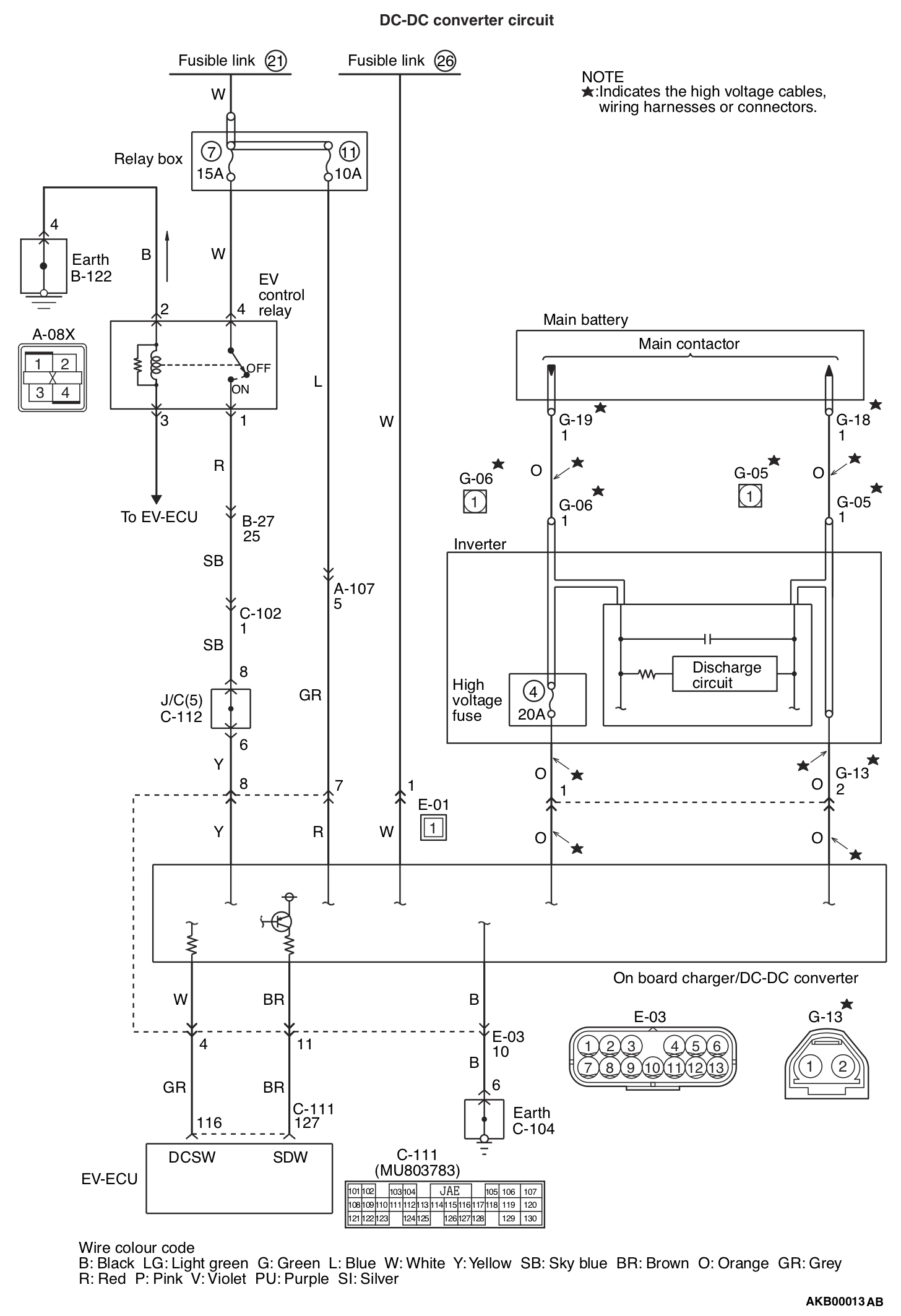
Modified the IC202 comparator drawing to add a common via path that was found linking several transistors and CN201 pin 6 which is the +12V switched input signal.
This common via seems to have a latching feature. If any of the transistor paths are true, then the drain path for the diodes is completed. After it starts then the diode path will be latched as long as the key switched 12V is applied.
What this means:
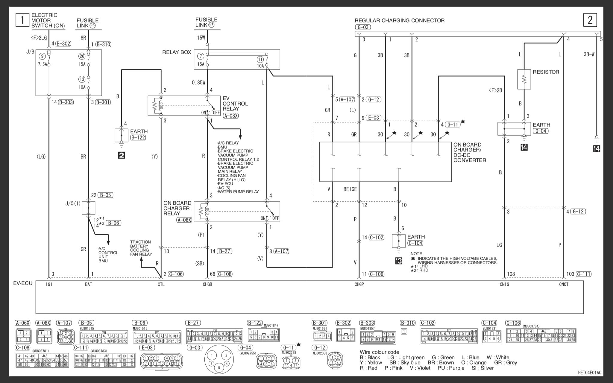
The DCDC can start and turn ON without a key-switched 12V (for example during EVVSE charging of the pack), but a key will keep it ON (such as while driving). This is the section of control logic that makes this possible.
Modified the IC202 comparator drawing to add a common via path that was found linking several transistors and CN201 pin 6 which is the +12V switched input signal.
This common via seems to have a latching feature. If any of the transistor paths are true, then the drain path for the diodes is completed. After it starts then the diode path will be latched as long as the key switched 12V is applied.
What this means:
The DCDC can start and turn ON without a key-switched 12V (for example during EVVSE charging of the pack), but a key will keep it ON (such as while driving). This is the section of control logic that makes this possible.