eldenh
Well-known member
It looks like I mislabeled the terminals. The central terminal of Q101, Q104 and Q110 are at 59v.
eldenh said:... I found that the ZD101 is at 2.56v and the output from D101 is 1.37v which is what i'm finding pin 11, VCC, of IC101. Since the spec sheet calls for 11.5 to 24v, it seems that ZD101 may be defective.
My understanding is that zener diodes below about 3.3 V are really useless, and even 5.1 V is a bit dodgy. So I doubt that it's a less than 1 V zener. More likely, the rest of the circuit is loading it down.kiev said:eldenh said:... I found that the ZD101 is at 2.56v and the output from D101 is 1.37v which is what i'm finding pin 11, VCC, of IC101. Since the spec sheet calls for 11.5 to 24v, it seems that ZD101 may be defective.
i tried to measure mine in-circuit--it was breaking over at about -0.5V, and had about 1V of forward drop. So your's is probably okay.
Ah, That's probably R117-R120 (51 kΩ x 4 = 204 kΩ). Perhaps consider shorting one or two of these temporarily.eldenh said:ZD101 is connected to the HV+ by about 205k.
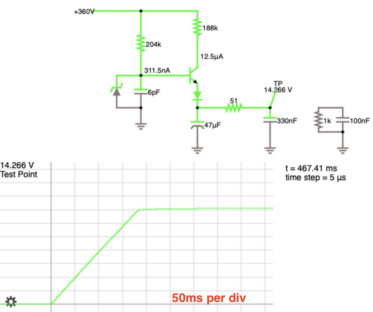
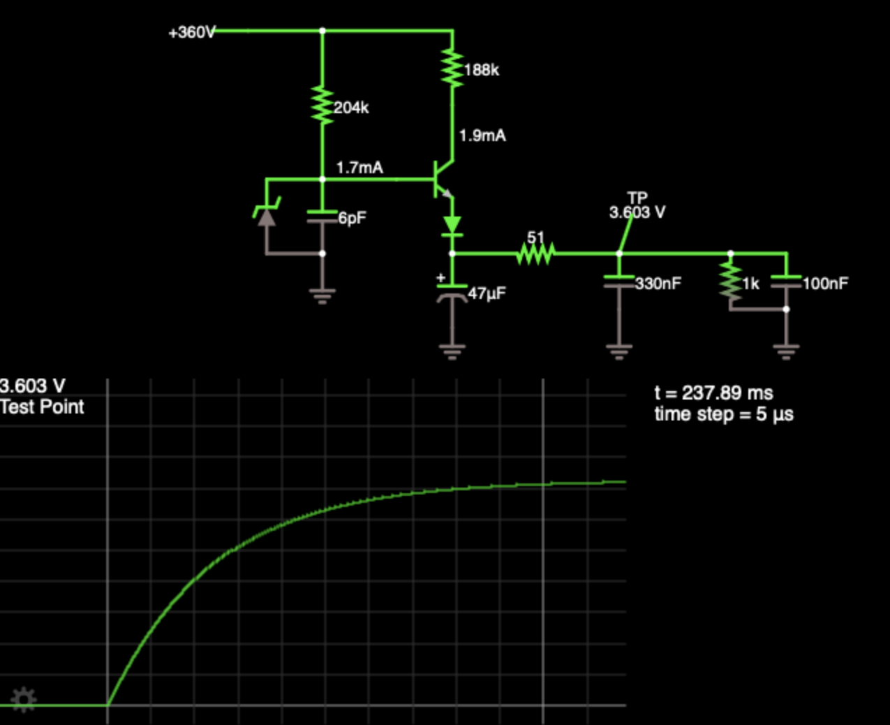
OK. So perhaps Q109 turning on, perhaps partially, is what "bootstraps" IC101. IC101 gets its power from the "logical OR" of Q109 or another path via another diode. That other path is probably one of the secondary windings of TX105, suitably rectified and filtered. So once IC101 is driving the MOSFET and transformer (probably actually a multi-winding inductor), it can power itself from the HV source. At that point, something will likely happen to turn off Q109. Perhaps there is a capacitor in the base circuit of that transistor that turns it off after a few hundred milliseconds.It appears the voltage out of Q109 is connected to VCC of IC101 by a diode.
Hopefully, that's a dumb battery charrger that doesn't need to see an actual battery there. Elcon charrgers for example won't turn on their output relay unless a battery is detected. An actual current limited power supply would be much better, since it can be programmed not to supply more than a few watts of power, which hopefully reduces the chances of something burning up. But of course, you have to work with what you have.Without proper test equipment, I've been making do with a 12v battery and a 58.7v bicycle battery charger.
coulomb said:OK. So perhaps Q109 turning on, perhaps partially, is what "bootstraps" IC101. IC101 gets its power from the "logical OR" of Q109 or another path via another diode. That other path is probably one of the secondary windings of TX105, suitably rectified and filtered. So once IC101 is driving the MOSFET and transformer (probably actually a multi-winding inductor), it can power itself from the HV source. At that point, something will likely happen to turn off Q109. Perhaps there is a capacitor in the base circuit of that transistor that turns it off after a few hundred milliseconds.It appears the voltage out of Q109 is connected to VCC of IC101 by a diode.
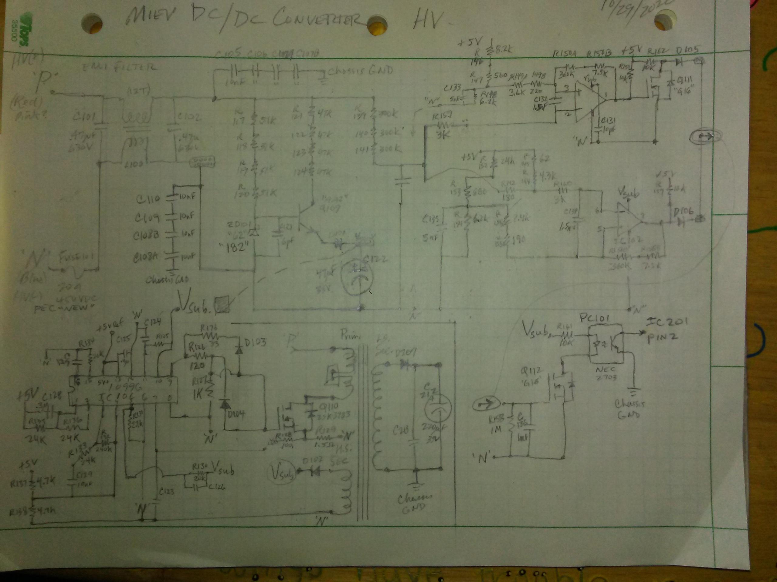
eldenh said:D103 reads 167 ohms both ways. C123 reads 104 ohms. I haven't checked the resistors yet and have been checking only the HV section initially. Most of the diodes in the Q101 to Q104 driver section appear to have a resistor in parallel. Q109 doesn't seem to be a junction transistor, the central lead checks as a diode to the left lead but always open to the right one.
Enter your email address to join: