The Troubleshooting and Repair for On-board Charger (OBC) Thread

Mitsubishi i-MiEV Forum

Help Support Mitsubishi i-MiEV Forum:

This site may earn a commission from merchant affiliate links, including eBay, Amazon, and others.
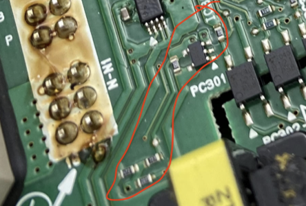
No that is not a TI chip it is JRC, i posted on the previous page that ic702 is a gate driver chip,
http://myimiev.com/forum/viewtopic.php?p=41344#p41352

i have a datasheet listed as NJM2369_E, which i could send you if you can't find it.

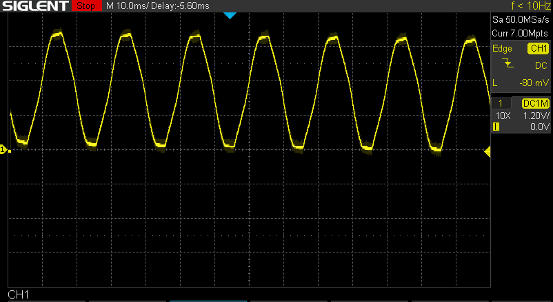
On which pins did you measure that 2.4 voltage? i assume you are powering the top board with the 12V power supply as before?
 
Oh, thank you very much!

I can measure nothing between OUT and GND and I do not even see anything with my oscilloscope there. FB is switching and between IN and GND I can measure no voltage.

KJ8doX2.png
 
i don't see the timebase or ch1 volts/div, but i'm guessing that it's 5V/div and it's hitting about 16V peak. And that is the FB signal, which is coming from the voltage reference ic318 and the resistor network on the other side of the board.

Swh7LtG.png


i'll study on that datasheet, but it seems that the ic702 is not working.

check optocoupler pc314, but if it is not working then no FB would get back to the ic702 from the ic318.

How about all the little passives, resistors and capacitors around ic702, pc314, and ic318?
 
I just checked the diode in PC314 and it reads fine. Should I desolder it to really test the component? All passives measure out fine in circuit and do not seem to be damaged even under a microscope.
 
This is the first time to ever have a failure like this, so it's a learning experience. i did a quick trace of this area some time ago but never drew up a schematic, but now i wish i had.

It's not clear if the FB signal on the scope was transferred from the VR chip ic318 on top thru the optocoupler [toshiba TLP127] then to the Gate driver chip ic702.
It appears to be a 50Hz signal, so i suspect it is picking up some stray electric field.

But if it is real, then the opto is probably okay, and you measured the photodiode as okay, which is what gets triggered by the VR output pulled up by the 16V on C845 and the little resistor network on pin 4 of ic318.

Can you take a reading on pin 4 of ic318, gnd is pin 5. Also what is the input voltage on pin 3?
 
I just realised that my oscilloscope probe was damaged and the measurements were wrong, since there was no GND connected. Sorry for that.

The FB line of IC702 is not switching and steady at 2.4V.

IC318 outputs nothing between REF (Pin 4) and ANODE (Pin 5)
 
Was there any voltage on the input, pin 3?

i found my original notes on tracing all this and will try to post a photo of them in case it might help, although it is not pretty.
 
I was just about to measure Pin 1 so I plugged in my power supply when I noticed that something has to be wrong. The supply displayed a too high power consumption at 2.747 W. I first thought, my wireing is wrong or I somewhere do have a short. I double checked everything and then I realised a current draw of 229mA, very similar to skykloggers original measurements.

After some measurements, TR310 is chopping again, and IC317 is producing a 5V rail! For the scope measurements in the post before I soldered small wires to the resistor of IC318 and I also measured the pins of IC702 the same way. I think there was a broken soldering joint which I accidentally fixed! I just took off all components regarding IC702/IC318 and resoldered them with good quality solder. The board seems to be fixed to me now.

Before I solder the waffle plate back on, should I take any pictures or measurements off the board for further reference?
 
that's great news. Would you be able to measure the voltage on the electrolytic caps, C845, C841 and C369?

And if not too much trouble the input and output of the VR, IC318?

If you were to guess or try to narrow it down to which resistors may have had the poor solder joint--the little one between pin 4 and 5 of IC318? the little one by C844 near IC702? Did you happen to get a picture of the area around IC702 after you pulled the waffle plate?

here are some notes from previous posts, not sure if they would have helped find this issue or not, but will repeat them for future troubleshooting:

There is a 330 Ohm resistor from pin 4 of ic702 to the gate of TR301. It has test point solder blobs on each end that you might be able to reach. Maybe it is open circuit?
and
IC702 (on bottom side) provides the gate drive for the FET, so it is likely not doing it's job. And IC318 (on upper side) provides the feedback signal to ic702, so it will be one or the other of those two chips, or some little passive component in those circuits, resistor, cap, diode, etc.

or bad solder joint of a passive.
 
Hello again,

I was not at home the last few days and I wanted to take the measurements for you. After turning the power supply on, I got the same problem as before. I did not even touch the boards and now they do not work anymore.

IC318 still measures nothing between pin 4 and pin 5. You mentioned to measure the input voltage on pin 1 but the datasheet states to me it is a NC pin and there is no voltage present there. Is IC318 a TI TL431-Q1?
 
What about on the capacitors listed previously--are they zeroed out too?

Maybe the voltage is not reaching the bottom board thru the ribbon cable--check the ribbon connection.

i will check if i have a listing of the voltages on each pin of the ribbon cable.

The issue could be on the top board power supplies created from the 12V input power?

Is there anyway to determine which +12V supply is not drawing current? CN101 pin 7 or pin 12, or how much is being drawn on each of those?

Here's some notes i had about the CN1 flat ribbon cable, not double checked:

pins 1-4: Ground, bottom of C841

pins: 16,18,20,31,33,40, 47-50 : Grounds

pins 5-8: +12V nominal, top side of C841

pins 12-13: 5V

pins 22-24: 5V to PC305

pin 25: RLY1 return
pins 26-29: RLY1 5V supply

pins 34-37: 16V nominal

pins 43-46: 5V
 
There are two 12V supplies to the top board of the OBC on CN101.
CN101 pin 7 is a Hot All The Time 12V Input supply.
CN101 Pin 12 is the Switched 12V supply labelled as "ICGC" on the board.

Hot All the Time:
From this Hot All The Time 12V, there is a 5V regulator on the top board, IC710, that creates a HAAT 5V feed on pins 22-24, which goes to PC305, an optocoupler that reports back on pin 21 the presence of the AC Input voltage downstream of the AC relay.

Switched:
The 12V on pins 5-8 of CN1 that shows up on C841 for the Transformer T302 circuit is coming from the Key ON Switched 12V feed from pin 12 of CN101.

The AC coil relay 5V supply on pins 26-29 is created from the Switched 12V supply.
 
Pin 13 of CN1 only outputs 1.92V but all other Pins seem to be fine.

The input on pin 7 consumes absolutely nothing, pin 1 consumes 125mA.
 
Your picture on page 53, looks like pin 7. Check resistor R748, there should be 5V there when powered up.

check you PM if you want to send me an email.
 
it looks like it is all around the switching of the transistor. The source comes from the top board 12V on pins 5-8.

i had thought ic318 may have come from one of the 5V supplies, but it also comes from the switching.

You might be able to trigger a response to come on by using either cold spray or hot air around the ceramic capacitors, e.g. C846 (meas. 884nF), and all those around ic702 in the power supply circuit, e.g. the timing cap on pin 7.

ICs won't heal themselves if they fail, but ceramic caps can crack and short out intermittently, especially with temperature changes. And try the Chips also, maybe there is an internal fault sensitive to temperature.
 
Back
Top